Dual-Ring Based Surface Plasmon Polaritons MIM Waveguide for High-Sensitivity Air Sensor
published: 8 November 2025 | https://doi.org/10.63174/xdi.NKFY5771
Abstract
Metal-insulator-metal (MIM) waveguides supporting surface plasmon polaritons (SPPs) offer a promising platform for refractive index sensing in air. However, limited sensitivity remains a major constraint for practical air-sensing applications. To obtain a high-sensitivity sensor, we propose a SPPs MIM waveguide sensor incorporating a tangent dual-ring resonator integrated with gain structure and waveguide strips. The proposed structure, fabricated on a silver substrate with air as the dielectric core, is systematically investigated using finite-difference time-domain (FDTD) simulations. By optimizing the structural parameters of the sensor model, the resonator exhibits continuous shifts in resonant wavelength as the refractive index varies from 1.00 to 1.05. A maximum sensitivity of 3540 nm/RIU is achieved. The findings demonstrate the potential of the designed sensor for highly accurate air quality monitoring, supporting the development of more effective environmental conservation strategies.
1. Introduction
Surface Plasmon Polaritons (SPPs) are electromagnetic surface waves generated by the resonance between incident photons and free electrons on the metal surface[1]. They break the diffraction limit, confine light within the nanoscale range, and thereby achieve subwavelength-scale transmission[2]. The intensity of the electromagnetic field decays exponentially in the direction perpendicular to the interface. At the metal-dielectric interface, SPPs generate a strong localized electromagnetic field[3-5]. This localized field enhancement effect regulates the optical field, creating conditions for the miniaturization and integration of photonic devices[6]. This is particularly true in cutting-edge fields such as nanophotonic sensing, optical communication, and surface-enhanced spectroscopy[7-9]. It enables the integration of core functional units, including waveguides, modulators, and sensors, onto chips at the micrometer or even nanometer scale, while providing critical physical foundations and technical support for emerging photonic systems[10].
Among various SPPs structures, the MIM waveguides exhibits better localized confinement of SPPs, confining most of the optical energy within the waveguide[11-13]. MIM waveguides are characterized by high optical confinement, low bending loss, and long propagation distance[14]. With the continuous research on MIM type SPPs waveguides, these waveguides have significant advantages in miniaturized circuits. They can support the realization of multifunctional devices such as optical filters, sensors, and optical switches[15-19], laying a foundation for the research on the coupling between MIM waveguides and resonant cavities.
In the research field of coupling between MIM waveguides and resonant cavities, cavity structures exhibit diversity, including semicircular rings[20], hexagons[21], L-shapes[22], and multi-tooth shapes[23]. Based on different resonant cavity structures, MIM waveguide-coupled resonant cavities can enhance the light-matter interaction and achieve ultra-sensitive detection of tiny refractive index changes[24-26]. Researchers have conducted extensive explorations. For example, Yang et al. proposed a square cavity above a straight waveguide, with a sensitivity of 1120 nm/RIU[27]; Wang et al. proposed a bilateral asymmetric equilateral triangular ring combined with a waveguide, achieving a sensitivity of 1149 nm/RIU[28]; Figuigüe M et al. proposed an MIM waveguide supplemented with a semi-elliptical ring resonator and a baffle, which exhibits a sensitivity of 1783 nm/RIU[29]; Ach S E et al. proposed a structure consisting of an eye-like defective resonator with nano wall side coupling, two slits, and waveguide, which exhibits a sensitivity of 3144 nm/RIU[30]. Investigations have revealed that the coupling of resonant cavities with different structures to waveguides has various functions, which can be used for detecting the composition of biological samples[31], as well as gas concentration[32] and temperature[33]. In these studies, sensitivity is a key focus, and there is still room for improvement in the sensitivity of existing structures.
We propose a tangent dual-ring waveguide sensor based on the SPPs MIM waveguide technology. This sensor is composed of tangent dual-ring resonators of identical size, semi rings gain structure and waveguide strips. Silver is used as the substrate material, and the waveguide strips are made of air. The FDTD is employed to simulate the propagation of electromagnetic waves. To optimize the sensor performance, the control variable method is used for quantitative parameter analysis of the sensor structure. By referring to the sensitivity and the shift of the resonant peak, the structural parameters are optimized and selected. Based on parameter adaptation, the refractive index of air was adjusted from 1.00 to 1.05, thus leading to a shift in the resonance peak. This opens up an innovative path for air quality detection and provides better technical support for precise detection.
2. Structural design
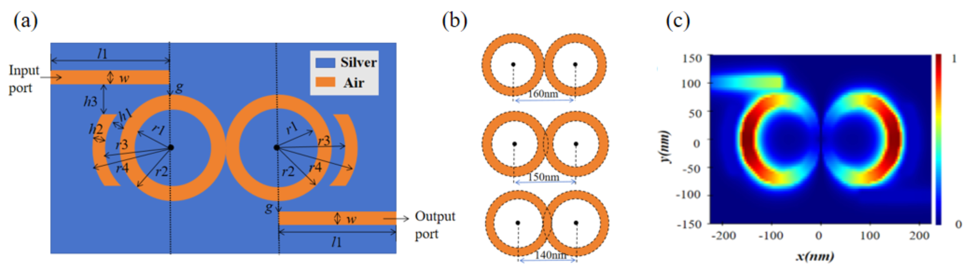
Figure 1. Structural design and resonance. (a) Schematic diagram of the MIM waveguide sensor. (b) The three configurations of dual-ring. (c) Magnetic field distribution.
Figure 1(a) presents the structural schematic of the sensor, which is composed of a tangent dual-ring resonator of identical size, semi circulars gain structure, and upper and lower straight waveguide strips. The inner (r1) and outer (r2) radii of the tangent-ring, as well as the inner (r3) and outer (r4) radii of the semi rings, are designed as concentric circles. In terms of material selection, the blue regions in the diagram represent silver, while the orange regions represent air. Silver is selected as the base material because it exhibits excellent plasmonic resonance properties in the visible and near-infrared regions, which can effectively enhance the local electromagnetic field[3-5]. Additionally, the dielectric constant of silver changes significantly with frequency[36]. Air acts as the insulating layer. The straight waveguide at the upper left acts as the input terminal for providing the light source, while the straight waveguide at the lower right is the output port used for exporting the light source. To present the specific structural details of the sensor more intuitively, the dimensional parameters of each component are also defined in the figure: l1 denotes the length of the waveguide strips, w represents the width of the waveguide strips, g is the gap between the waveguide strips and the dual-ring, h1 is the gap between the dual-ring and the semi rings, h2 is the width of the semi rings, and h3 is the gap between the semi rings and the waveguide strips. The specific parameters are as follows: l1 = 320 nm, r1 = 60 nm, r2 = 80 nm, r3 = 100 nm, r4 = 120 nm, w = 18 nm, g = 10 nm, h1 = 20 nm, h2 = 20 nm, and h3 = 30 nm. These parameters lay a foundation for the precise fabrication and performance regulation of the sensor.
3. Method
We employed the FDTD to simulate the propagation and interaction of electromagnetic waves[37] , which was utilized to conduct sensing research on the relevant MIM waveguide structure. To thoroughly investigate the characteristics of the sensor, a two-dimensional simulation was conducted. Monitors were respectively positioned at the input and output ports to monitor the incident efficiency and output efficiency. Transmittance was defined as the ratio of output optical power to input optical power, that is Transmittance = Pout/Pin[38]. The boundary conditions around the computational domain are set to perfectly matched layers (PML) to absorb the outgoing electromagnetic waves. Through the simulation, the magnetic field energy distribution was obtained.
As shown in Figure 1(c), which presents the magnetic field distribution, the dual-ring structure serves as the core sensing element where energy is highly localized at both symmetric sides, as indicated by the color bar. The dual-ring structure serves as the core part of the sensor, with energy highly concentrated on the symmetrical sides of the rings, forming distinct bright regions. This phenomenon is closely related to the SPPs resonant condition: under resonant modes, the propagation path of light is specific, and stable resonant can only be formed when the specific phase-matching condition is satisfied. This resonance condition[39] is expressed as:
λres=2ƖeƒƒRe(ոeƒƒ)/(N - φ/π), “N = 1,2,3...” (1)
where Ɩeƒƒ denotes the propagation length of SPPs in the waveguide, φ represents the phase shift caused by the reflection of SPPs from the surface of the cavity metal, Re(ոeƒƒ) stands for the real part of the effective refractive index, and N indicates the order of standing wave resonance.
At positions satisfying the resonant condition, the optical field continuously superimposes and intensifies to form bright spots. In contrast, at positions not meeting the resonance condition, the optical field exhibits phase mismatch, leading to weakened mutual interference and the formation of dark spots. These results confirm that the dual-ring structure satisfies the SPPs resonant condition, the incident electromagnetic waves resonate with free electrons on the metal surface, causing the optical field to continuously superpose and strengthen inside the rings, thereby forming the bright regions.
In terms of function analysis, sensitivity is a key indicator for evaluating the sensor’s response to refractive index changes. It is defined as the ratio of the resonant wavelength shift (Δλ) to the change in the refractive index of the surrounding medium (Δn)[40], expressed as:
S=Δλ/Δn (2)
By capturing the subtle shift of the resonant wavelength with the ambient refractive index, the sensor’s ability to detect changes in the surrounding medium can be intuitively reflected. A larger sensitivity value indicates that the sensor is more responsive to tiny refractive index fluctuations, making it a core parameter for assessing sensor performance.
4. Structural Parameter Optimization and Analysis
In this study, the proposed dual-ring structure was precisely controlled by adjusting the positional relationship between the ring centers, resulting in three distinct configurations: tangent, intersection, and overlap. The distance between the centers of the two rings, denoted as d, served as the key parameter for modifying the effective resonant region. Specifically, d = 160 nm corresponds to a tangent configuration, where the outer radii of the rings are tangent to each other; d = 150 nm represents an intersecting configuration, with an overlap of 10 nm occurring between the outer and inner radii; and d = 140 nm indicates a overlap configuration, where the rings overlap by 20 nm and their inner radii become tangent. The three structural forms are shown in Figure 1(b).
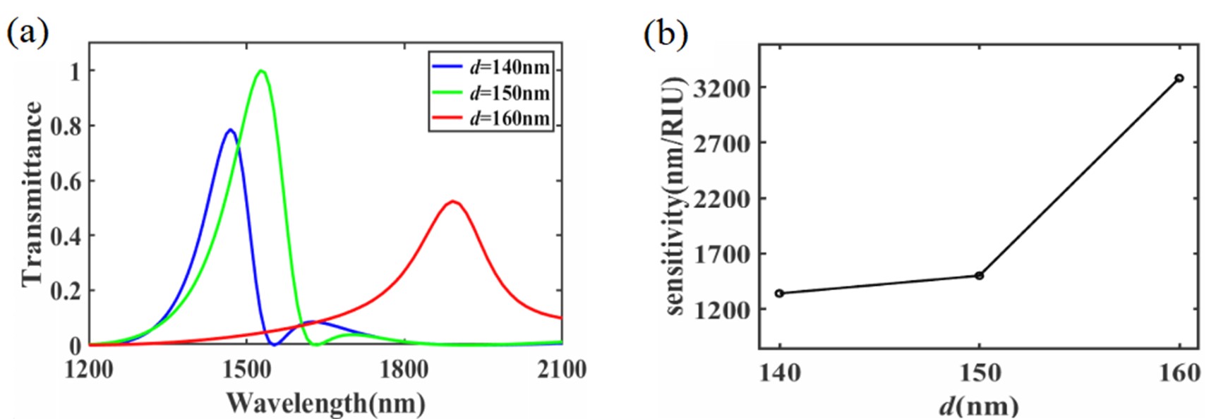
Figure 2. Resonance and sensitivity correspond to distinct d. (a) Resonant wavelengths with different distances d in dual-ring structure. (b) Sensitivity with different distances d in dual-ring structure.
Figure 2(a) displays the resonant peak wavelengths for the tangent, intersection, and overlap morphological configurations of the dual-ring structure. The blue, green and red curves correspond to the dual-ring structures with centers distance d = 140 nm, 150 nm, and 160 nm, respectively, with their resonant peaks centered around 1450 nm, 1600 nm, and 1950 nm. A redshift of the resonant peak is observed with increasing d. The observed resonant peak wavelengths shift results from geometric modifications to the dual-ring structure induced by changes in d. When d = 140 nm, the two rings overlap extensively. In this scenario, the propagation paths of SPPs overlap significantly, severely compressing the effective propagation space. When d = 150 nm, the two rings have a partial overlap, the propagation paths of SPPs intersect and partially overlap in the overlapping region, this partial overlap compresses the effective propagation space. When d = 160 nm, the two rings are tangent without any overlapping area. In this case, SPPs propagate along the circumferential path of each ring independently. The propagation path is highly intact, with no mutual interference or overlap, allowing SPPs to travel along the full circumference of each ring. Specifically, a larger d reduces the overlapping area between the rings, resulting in a longer effective propagation length Ɩeƒƒ for SPPs within the cavity. As described by the resonance condition in Equation (1), an increase in Ɩeƒƒ exhibits a direct positive correlation with resonant wavelength λres, thereby inducing the observed redshift phenomenon.
Figure 2(b) presents the sensitivity corresponding to the centers distance d of the dual-ring. The results depicted in the Figure 2(b) demonstrate that the sensitivities corresponding to d = 140 nm, d = 150 nm, and d = 160 nm are quantified as 1430 nm/RIU, 1500 nm/RIU, and 3280 nm/RIU, respectively. The sensitivity shows a non linear relationship with the increase of d. From the trend of the polyline, when d is in values of 140 and 150 nm, the sensitivity increases relatively slowly. However, when d reaches 160 nm, the sensitivity rises significantly. These results indicate that changes in the rings distance d have a significant impact on sensitivity, the dual-ring structure attains its maximal sensitivity under the tangent state, with sensitivity progressively decreasing as overlap occurs.
Following confirmation of the dual-ring tangent configuration as the optimal state, we employed the method of cotrolling variables to optimize the structural parameters. Firstly, the width of the upper and lower straight waveguides was adjusted, starting from 18 nm, the waveguide strips width w were increased in increments of 2 nm up to 22 nm, and its effects on the resonance characteristics and sensitivity were analyzed.
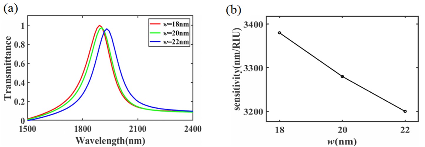
Figure 3. Resonance and sensitivity correspond to the waveguide strips width w. (a) Resonant wavelengths with different w in dual-ring structure. (b) The sensitivity corresponding to different w values.
Figure 3(a) shows the resonant wavelengths corresponding to different waveguide strips width w under the same refractive index. In the Figure 3(a), the red, green, and blue curves correspond to w = 18 nm, 20 nm, and 22 nm, respectively. All resonant peaks for the investigated w are observed to cluster around 1900 nm. And as w increases, the resonant peak undergoes a redshift along the wavelength axis. Increasing w expands the propagation cross section of electromagnetic waves within the waveguide, which in turn induces an increase in the real part of the effective refractive index Re(ոeƒƒ) of SPPs. As the resonant wavelength is proportional to Re(ոeƒƒ), this increment in Re(ոeƒƒ) leads to a corresponding increase in the resonant wavelength, ultimately manifesting as a redshift. The vertical axis of the Figure 3(a) denotes transmittance. Notably, the transmittance curve attains its maximum peak value at w = 18 nm, a phenomenon that signifies optimal coupling efficiency between the waveguide and the resonant cavity. As illustrated in Figure 3(b), sensitivity exhibits a monotonic downward trend with increasing w, it registers 3380 nm/RIU at w = 18 nm, declines to approximately 3250 nm/RIU at w = 20 nm, and further drops to around 3150 nm/RIU at w = 22 nm. These findings confirm that w exerts a tangible influence on sensitivity. Specifically, at w = 18 nm, the sensor demonstrates the highest responsiveness to refractive index variations, thereby establishing this as the optimal waveguide strip width.
Building on the optimal parameter of w, adjustments were made to the structural parameter of the inner ring radii r1, starting from 50 nm, r1 was incrementally increased by 5 nm up to 65 nm, with the corresponding effects of this parameter on resonant characteristics and sensitivity systematically analyzed. Variations in r1 are found to directly modulate the effective interaction region of the resonant structure. In the initial structure, r1 is 60 nm; a reduction in r1 expands the effective resonant region, whereas an increase in r1 leads to its contraction.
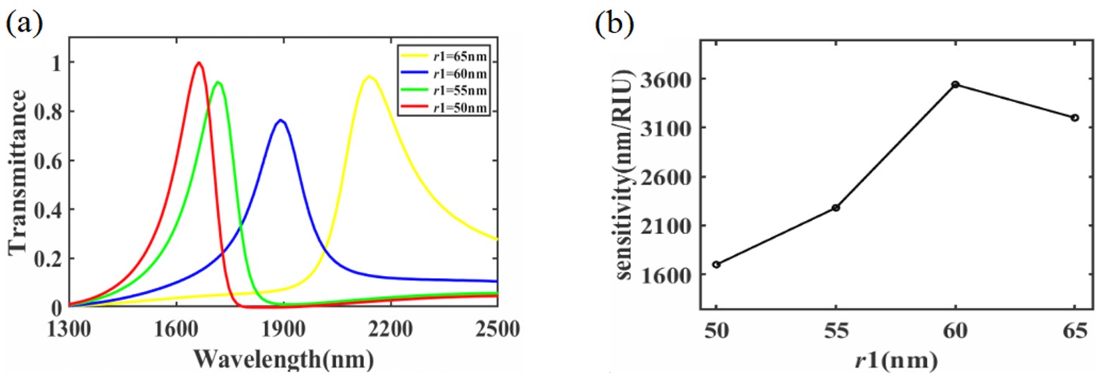
Figure 4. Resonance and sensitivity correspond to the inner ring radii r1. (a) Resonant wavelengths with different r1 in dual-ring structure. (b) The sensitivity corresponding to r1.
As shown in Figure 4(a), it presents the resonant wavelengths corresponding to the inner radii r1 of the dual-ring. In the Figure 4(a), the red, green, blue, and yellow curves correspond to the dual-ring structures with inner radii r1 = 50 nm, 55 nm, 60 nm, and 65 nm, respectively, with their resonant peaks centered around 1600 nm, 1700 nm, 1900 nm, and 2200 nm. A redshift of the resonant peak is observed with increasing r1.
A clear redshift of the resonant peak is observed with increasing r1. This shift originates from two key effects of r1 increment. On one hand, it induces contraction of the dual-ring’s effective resonant region, shortening the propagation path of SPPs within the structure; on the other hand, it alters the dual-ring’s curvature, which in turn reduces the phase shift φ. Since a decrease in φ drives an increase in resonant wavelength, the observed redshift follows.
Figure 4(b) illustrates sensitivity variations corresponding to different inner radii r1 of the dual-ring. From the Figure 4(a), sensitivity dependent on r1 exhibits a nonlinear trend of first increasing and then decreasing, it measures approximately 1700 nm/RIU at r1 = 50 nm, rises to 2100 nm/RIU at r1 = 55 nm, peaks at 3500 nm/RIU at r1 = 60 nm, and subsequently declines to 3100 nm/RIU at r1 = 65 nm. This indicates that the effective resonant region has a significant impact on resonance and sensitivity. The sensitivity reaches the maximum when r1 = 60 nm. With a further increase in r1, the coupling strength between the optical field and the resonant structure weakens, resulting in a decrease in sensitivity. Therefore, r1 = 60 nm is determined as the optimal inner radius of the dual-ring.
On the basis of determining the inner radius of the dual-ring, change the distance h3 from the waveguide strips to the semi rings gain structure, increasing h3 from 20 nm in steps of 10 nm up to 50 nm, so as to analyze the influence of this parameter on the resonance characteristics and sensitivity.
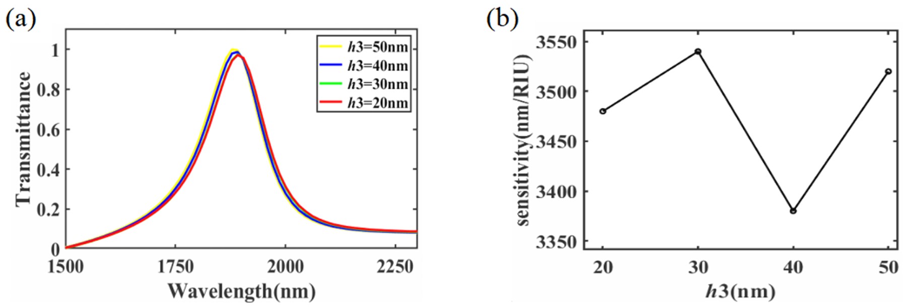
Figure 5. Resonance and sensitivity correspond to the distance h3. (a) The resonant wavelength corresponding to the distance h3 from the waveguide strips to the semi rings gain structure. (b) The corresponding sensitivity of h3.
As shown in Figure 5(a), the resonant wavelengths corresponding to h3 are presented. In the Figure 5(a), the red, green, blue, and yellow curves correspond to the spacing h3 = 20 nm, 30 nm, 40 nm, and 50 nm, respectively. A close examination reveals that the discrepancies in resonant wavelength across different h3 values are relatively modest, with all peaks clustering around 1900 nm. This suggests that h3 exerts only a weak influence on both the resonant peak position and the coupling efficiency. To analyze the optimal structural parameters, the sensitivity of h3 can be referenced, as illustrated in Figure 5(b). Analysis shows that the sensitivity exhibits fluctuations with variations in h3: it measures approximately 3470 nm/RIU at h3 = 20 nm, increases to around 3540 nm/RIU when h3= 30 nm, then declines to roughly 3370 nm/RIU at h3 = 40 nm, and rises again to about 3500 nm/RIU at h3 = 50 nm. On this basis, the coupling effect reaches its optimum at h3 = 30 nm, and the device also demonstrates higher sensitivity in response to refractive index variations under this condition.
Further adjustments were made to h1 the distance between the dual-ring and the semi rings gain structure with h1 increased in 5 nm increments from an initial value of 15 nm up to 25 nm. This parameter tuning was conducted to investigate the impact of h1 on the resonant characteristics and sensitivity of the device.
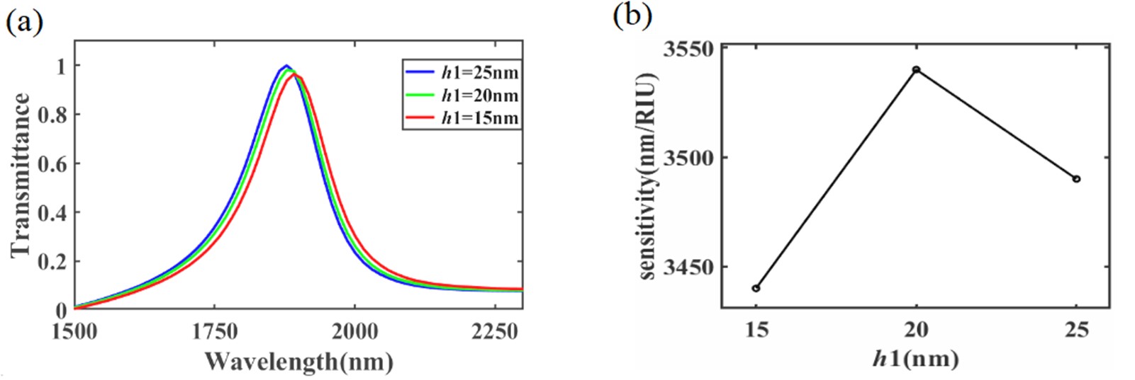
Figure 6. Resonance and sensitivity correspond to the distance h1. (a) The resonance wavelength corresponding to the distance h1 of the dual-ring to semi rings gain structure. (b) The sensitivity corresponding to h1.
Figure 6(a) delineates the optical response profiles corresponding to different spacing values h1 between the dual-ring and semi rings gain structure, where the red, green, and blue curves are assigned to h1 = 15 nm, 20 nm, and 25 nm, respectively. A salient observation extracted from these profiles is that as h1 increases incrementally, all resonant predominantly localized within the wavelength window of 1800 nm to 1900 nm undergo a discernible blueshift, reflecting the modulation of h1 on the resonant behavior of the structure. An incremental increase in h1 attenuates the inter structural coupling interaction between the dual-ring and semi rings, a phenomenon that directly diminishes the gain transferred from the semi rings to the dual-ring. This coupling attenuation induces two effects: a reduction in the effective local field intensity of the dual-ring, and a concomitant decrease in the real part of the effective refractive index Re(ոeƒƒ) for SPPs. As dictated by the resonance condition outlined in Equation (1), the resonant wavelength exhibits a proportional relationship with Re(ոeƒƒ); thus, the reduction in directly translates to a decrease in the resonant wavelength, manifesting as a distinct blueshift. Figure 6(b) demonstrates that the sensitivity of the h1 exhibits a non-monotonic trend with the increase in h1,a trend characterized by a measurement of approximately 3530 nm/RIU at h1 = 15 nm, a rise to roughly 3540 nm/RIU at h1 = 20 nm, and a subsequent drop to approximately 3500 nm/RIU at h1 = 25 nm. Collectively, these observations indicate that h1 = 20 nm represents the optimal structural parameter, as it enables the structure to simultaneously achieve a sensitive response to refractive index fluctuations, high sensitivity, and efficient coupling between the dual-ring and semi rings gain components.
On the basis of optimizing h1, we will further adjust the width h2 of the semi rings gain structure, increasing h2 from 15 nm in steps of 5 nm up to 25 nm, to analyze the influence of this parameter on the resonance characteristics and sensitivity.
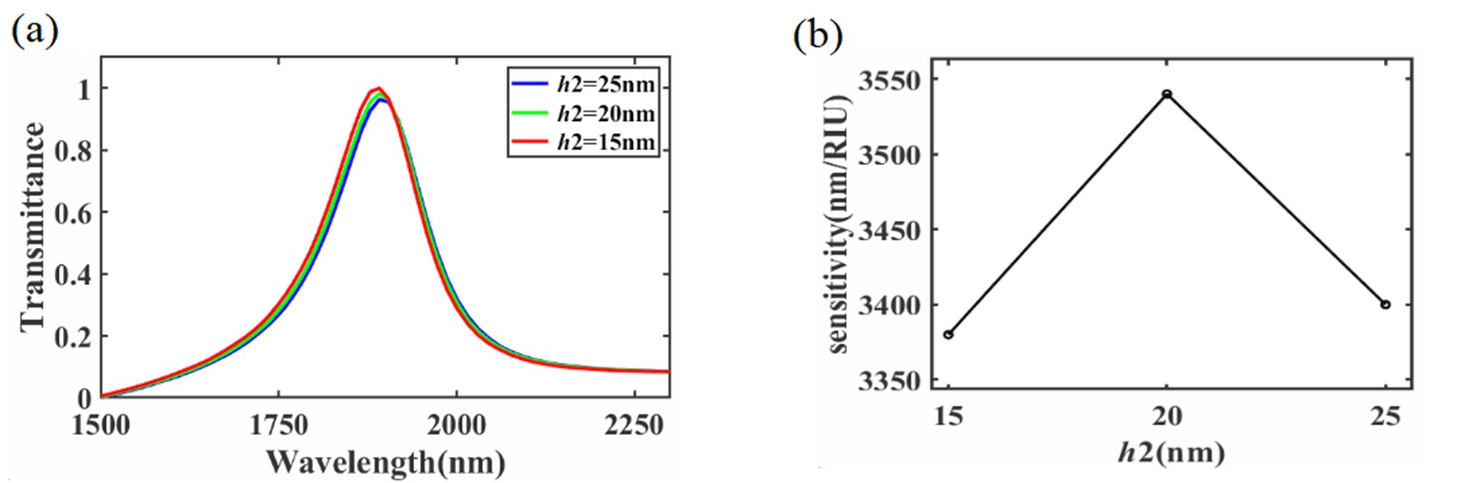
Figure 7. Resonance and sensitivity correspond to the distance h2. (a) The resonant wavelength corresponding to the width h2 of the semi rings gain structure. (b) The sensitivity corresponding to h2.
As shown in Figure 7(a), The red, green, and blue curves correspond to the semi-rings with a width h2 = 15 nm, 20 nm, and 25 nm, respectively. A key observation from the curves is that as h2 increases, the resonant wavelength between 1800 nm and 1900 nm redshift progressively. As delineated in Figure 7(b), the sensitivity exhibits a non-monotonic trend of initial enhancement followed by attenuation with the incremental increase in h2, it registers approximately 3380 nm/RIU at h2 = 15 nm, peaks at roughly 3540 nm/RIU when h2 = 20 nm, and subsequently declines to approximately 3400 nm/RIU at h2 = 25 nm. The width h2 dictates the thickness of the gain medium and its coupling efficiency with SPPs in the dual-ring resonator. When h2 = 20 nm, the gain medium achieves optimal mode matching with SPPs, this thickness is sufficient to enable stimulated emission for compensating SPPs’ intrinsic metal loss in the silver substrate, thereby extending the effective propagation length of SPPs, thus establishing h2 = 20 nm as a structural parameter that ensures superior coupling performance of the entire dual-ring and semi rings gain structure.
5. Simulation results analysis
After the systematic optimization of the structural parameters mentioned above, we conducted a simulation of the sensing performance of the sensor. Specifically, we adjusted the refractive index of air from 1.00 to 1.05 with a step size of 0.01, aiming to analyze the variation patterns of the resonant wavelength and sensitivity.
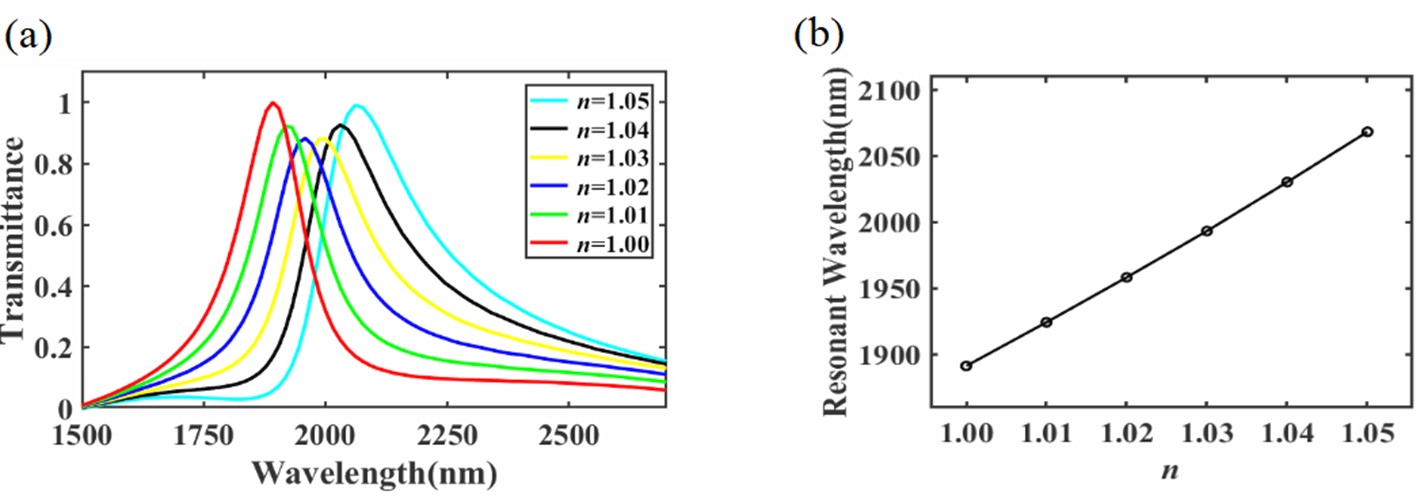
Figure 8. The resonant wavelength shift of n and the corresponding values. (a) The resonant wavelength shift of the sensor with the n range of 1.00 to 1.05. (b) The wavelengths corresponding to the resonant wavelength at different n.
In Figure 8(a), the six curves, spanning from red to cyan, correspond to air refractive index values ranging from 1.00 to 1.05. A notable observation is that as the n increases, resonant wavelength exhibits a distinct redshift, with specific values as follows, 1850 nm at n = 1.00, 1900 nm at n = 1.01, 1950 nm at n = 1.02, 2000 nm at n = 1.03, 2050 nm at n = 1.04, and 2100 nm at n = 1.05. An increase in the n alters the propagation environment of SPPs, thereby inducing an increase in the real part of the effective refractive index Re(ոeƒƒ) of SPPs. As dictated by the resonance condition outlined in Equation (1), the resonant wavelength is proportional to Re(ոeƒƒ). Consequently, a rise in Re(ոeƒƒ) triggers a commensurate increase in the resonant wavelength, manifesting as the observed redshift.
Figure 8(b) presents the relationship between resonant wavelength and varying n. The horizontal axis denotes the variable n, spanning 1.00 to 1.05, while the vertical axis denotes the resonant wavelength, ranging from 1850 nm to 2050 nm. Evident this Figure 8(b) is that the resonant wavelength exhibits a positive linear correlation with the n and this correlation is consistent with the resonant peak wavelength values presented in Figure 8(a). The slope can be calculated from Figure 8(b), and according to Equation (2), the slope represents the sensitivity. The calculated sensitivity is 3540 nm/RIU.
6. Conclusions
This study design a tangent dual-ring sensor based on SPPs MIM waveguide for air refractive index detection. The sensor consists of a tangent dual-ring resonant cavity, semi rings gain structure and straight waveguides strips, achieving high-sensitivity sensing through the coupling between the resonant cavity and the waveguides. Through systematic research on the dual-ring structure, namely the distance d between the dual-ring centers, the structural parameters include the waveguide strips width w, the inner radius r1 of the dual-ring, the distance h3 between the waveguide strips and the semi rings, the width h2 of the semi rings, the distance h1 between the semi rings and the dual-ring, and the influence of the air refractive index on the sensing performance. We conclude that the dual-ring in the tangent state with d = 160 nm represent the optimal position structure, where the sensitivity is significantly higher than that at d = 150 nm and d = 140 nm. The optimal combination of structural parameters are determined as w = 18 nm, r1 = 60 nm, h3 = 20 nm, h2 = 20 nm, and h1 = 20 nm. Two-dimensional simulation results show that within the air refractive index range of 1.00 to 1.05, the resonant wavelength has a linear positive correlation with the refractive index. Finally, calculations yield the key conclusion, the sensitivity reaches a maximum of 3540 nm/RIU, enabling the accurate detection of tiny refractive index changes. The investigated range from 1.00 to1.05 targets extreme air pollution scenarios: for PM2.5 pollution, during severe haze events, the effective refractive index of air-particle mixtures can rise to above 1.005[41], this range covers the refractive index fluctuation interval of air in real-world extreme pollution events, catering to performance evaluation for environmental emergency monitoring. This sensor holds broad prospects in the field of nano optical sensing, and is particularly suitable for air quality monitoring and trace analysis of biological samples. It provides a new solution for the development of environment monitoring and precision sensing technologies.
Author Contributions
Fei Zhao: Conceptualization, Investigation, Writing – original draft, Writing – review & editing. Ting Cui: Visualization, Writing – review & editing. Wenxian He: Investigation, Data curation. Miaomiao Chen and Huili Pei: Analysis, Validation. Meng Zhang: Methodology, Formal analysis. Li Ma: Conceptualization, Writing – review & editing, Supervision, Project administration.
Acknowledgment
This research was funded by Scientific and Technological Innovation Programs of Higher Education Institutions in Shanxi (STIP) (2024L349, 2022L514).
Conflict of Interest
The author Li Ma is an editor of X-Disciplinarity but was not involved in the peer review or decision-making process for this article.
References
-
T. K. Sarkar, M. N. Abdallah, M. Salazar-Palma, W. M. Dyab. "Surface Plasmons-Polaritons, Surface Waves, and Zenneck Waves: Clarification of the terms and a description of the concepts and their evolution." IEEE Antennas Propag. Mag. 2017, 59, 3, 77-93.
-
W. L. Barnes, A. Dereux, T. W. Ebbesen. "Surface plasmon subwavelength optics." Nature. 2003, 424, 6948, 824-830.
-
H. J. Zhao, J. S. Du, S. W. Wang, X. Wang, T. Q. Zhang, R. T. Yu, Z. T. Chi, B. Wang. "Triple narrow-spectrum enhanced multiparameter sensor based on asymmetric MIM waveguide for gas and liquid sensing." Opt Las Technol. 2024, 175, 110754.
-
L. Yang, J. C. Wang, L. Z. Yang, Z. D. Hu, X. J. Wu, G. G. Zheng. "Characteristics of multiple Fano resonances in waveguide-coupled surface plasmon resonance sensors based on waveguide theory." Sci Rep. 2018, 8, 2560.
-
W. J. Choi, Y. H. Jo, J. M. Ahn, E. S. Seo, Q. H. Park, Y. M. Jhon, W. S. Choi. "Control of randomly scattered surface plasmon polaritons for multiple-input and multiple-output plasmonic switching devices." Nat Commun. 2017, 8, 14636.
-
X. B. Ren, K. Ren, Y. X. Cai. "Tunable compact nanosensor based on Fano resonance in a plasmonic waveguide system." Appl Opt. 2017, 56, 31, H1-H9.
-
A. A. Rifat, M. R. Hasan, R. J. Rajib, A. E. Miroshnichenko. "Microstructured optical fiber-based plasmonic sensors." Comput Photonic Sensors. 2018, 203-232.
-
T. Ioannidis, T. Gric, E. Rafailov. "Controlling Surface Plasmon Polaritons Propagating at the Boundary of Low-Dimensional Acoustic Metamaterials." Appl. Sci. 2021, 11, 14, 6302.
-
M. Xia, P. Zhang, K. Qiao, Y. Bai, Y. H. Xie. "Coupling SPP with LSPR for Enhanced Field Confinement: A Simulation Study." J. Phys. Chem. C. 2015, 120, 527-533.
-
G. Y. Li, J. S. Zhang. "Ultra-broadband and efficient surface plasmon polariton launching through metallic nanoslits of subwavelength period." Sci Rep. 2014, 4, 5914.
-
F. Chen, H. F. Zhang, L. H. Sun, C. C. Yu. "Liquid crystal based tunable triple Fano resonance in resonator waveguide coupled with a defect." Optik. 2020, 212, 164755.
-
S. L. Li, Y. L. Wang, R. Z. Jiao, L. L. Wang, G. Y. Duan, L. Yu. "Fano resonances based on multimode and degenerate mode interference in plasmonic resonator system." Opt. Express. 2017, 25, 4, 3525-3533.
-
F. Chen, H. F. Zhang, L. H. Sun, J. J. Li, C. C. Yu. "Temperature tunable Fano resonance based on ring resonator side coupled with a MIM waveguide." Opt Las Technol. 2019, 116, 293-299.
-
Y. H. Fang, K. H. Wen, Y. W. Qin, Z. F. Li, B. Y. Wu. "Multiple Fano resonances in an end-coupled MIM waveguide system." Opt Commun. 2019, 452, 12-17.
-
X. Y. Yang, X. Y. Hu, Z. Chai, C. C. Lu, H. Yang, Q. H. Gong. "Tunable ultracompact chip-integrated multichannel filter based on plasmon-induced transparencies." Appl. Phys. Lett. 2014, 104, 22, 221114.
-
C. H. Wu, Z. C. Guo, S. X. Chen, J. Yang, K. H. Wen. "Refractive index sensing based on multiple Fano resonances in a plasmonic defective ring-cavity system." Results Phys. 2021, 27, 104508.
-
H. Y. Zhang, D. L. Shen, Y. P. Zhang. "Circular split-ring core resonators used in nanoscale metal-insulator-metal band-stop filters." Laser phys. Lett. 2014, 11, 115902.
-
S. Paul, M. Ray. "Multispectral switching using Fano resonance and plasmon-induced transparency in a plasmonic waveguide-coupled resonator system." Plasmonics. 2019, 14, 1113-1122.
-
J. F. Chen, J. Li, X. Liu, S. Rohimah, H. Tian, D. W. Qi. "Fano resonance in a MIM waveguide with double symmetric rectangular stubs and its sensing characteristics." Opt Commun. 2021, 482, 126563.
-
Y. F. C. Chau. "Enhanced plasmonic waveguide sensing performance with a semicircular-ring resonator." Micro Nano Struct. 2023, 174, 207469.
-
P. Gu, H. J. Yang, D. Q. Li, H. Q. Zhu, J. Chen, Z. X. Zhang, Z. D. Yan, C. J. Tang, F. X. Liu, Z. Chen. "High-Q and Intense Lattice Plasmon Resonance in Hexagonal Nonclose Packed Thin Silver Nanoshells Array." J. Phys. Chem. C. 2024, 128, 15, 6161-6502.
-
T. S. Chen, J. Y. Gao, X. X. Wang, Y. Z. Chen, H. Yang, Y. P. Qi. "High FOM fano resonance refractive-index sensor based on a baffled MIM waveguide coupled with an inverted L-Shaped resonator." Phy. Scripta. 2024, 100, 015533.
-
J. Tao, X. G. Huang, X. S. Lin, Q. Zhang, X. P. Jin. "A narrow-band subwavelength plasmonic waveguide filter with asymmetrical multiple-teeth-shaped structure." Opt Express. 2009, 17, 16, 13899-13904.
-
C. T. C. Chao, Y. F. C. Chau, S. H. Chen, H. J. Huang. "Ultrahigh Sensitivity of a Plasmonic Pressure Sensor with a Compact Size." Nanomaterials. 2021, 11, 11, 3147.
-
C. T. C. Chao, Y. F. C. Chau. "Highly Sensitive Multichannel Fano Resonance-Based Plasmonic Sensor for Refractive Index and Temperature Sensing Application." Photonics. 2023, 10, 1, 82.
-
X. J. Rao, X. X. Wang, Y. Z. Chen, H. W. Chen, Y. P. Qi, H. Yang. "Highly sensitive self-referential plasmonic sensor based on double-layer nested grating." Opt Commun. 2024, 558, 130348.
-
Z. Chen, Y. L. Yu, Y. Y. Wang, N. Guo, L. Xiao. "Compact plasmonic structure induced mode excitation and Fano resonance." Plasmonics. 2020, 15, 2177-2183.
-
J. C. Wang, H. L. Feng, J. Y. Zhang, C. Liu, Z. X. Zhang, D. C. Fang, L. H. Wang, Y. Gao. "Plasmonic band-stop MIM waveguide filter based on bilateral asymmetric equilateral triangular ring." Optik. 2022, 265, 169535.
-
M. Figuigue, O. Mahboub, R. E. Haffar. "Optical Properties of Multiple Fano Resonance in MIM Waveguide System Coupled with a Semi-Elliptical Ring Resonator." Plasmonics. 2024, 19, 721-732.
-
S. E. Achi, A. Hocini. "Multiple Fano resonance modes in an ultra-compact plasmonic waveguide-cavity system for temperature sensing." Results Phys. 2023, 55, 747.
-
H. L. Feng, J. Y. Zhang, Z. X. Zhang, D. C. Fang, J. C. Wang, C. Liu, T. Wu, G. Wang, L. H. Wang, L. L. Ran, Y. Gao. "Design of nanorod- embedded bandstop MIM waveguide filters with high filtering efficiency and sensitivity." Opt Commun. 2022, 510, 127957.
-
J. H. Chen, L. Wang, Y. T. Feng, J. X. Chen, Y. P. Zeng. "A nano-refractive index sensor based on a MIM waveguide with a semicircular ring rectangular resonator." Micro Nano Struct. 2024, 186, 207730.
-
S. Kenmotsu, M. Hirasawa, T. Tamadate, C. Matsumoto, S. Osone, Y. Inomata, T. Seto. "Surface-Enhanced Raman Scattering on Size-Classified Silver Nanoparticles Generated by Laser Ablation." ACS Omega. 2024, 9, 36, 37418-38315
-
Y. F. Ye, J. Y. Y. Loh, A. Flood, C. Y. Fang, J. Chang, R. Z. Zhao, P. Brodersen, N. P. Kherani. "Plasmonics of Diffused Silver Nanoparticles in Silver/Nitride Optical Thin Films." Sci Rep. 2019, 9, 20227.
-
T. Wu, Y. M. Liu, Z. Y. Yu, Y. W. Peng, C. G. Shu, H. Ye. "The sensing characteristics of plasmonic waveguide with a ring resonator." Opt Express. 2014, 22, 7, 7669-7677.
-
T. Afdol, M. O. Faruque, R. A. Mahmud, R. H. Sagor, A. K. Nahin, M. A. A. Aumi, K. M. S. Hasan, S. Sazid, N. M. N. Nasser. "Numerical analysis of an asymmetric hexagonal plasmonic refractive index sensor model based on metal–insulator–metal and Si-insulator–Si waveguide." Sens Bio-Sens Res. 2023, 40, 100563.
-
J. Zhu, G. Wang. "Sense high refractive index sensitivity with bragg grating and MIM nanocavity." Results Phys. 2019, 15, 102763.
-
H. Wei, X. R. Tian, D. Pan, L. Chen, Z. L. Jia, H. X. Xu. "Directionally-Controlled Periodic Collimated Beams of Surface Plasmon Polaritons on Metal Film in Ag Nanowire/Al2O3/Ag Film Composite Structure." Nano Lett. 2015, 15, 1, 560-564.
-
Y. Shangbo, J. Zhu, J. G. Yin. "Analysis of the water-soluble vitamins based on MIM waveguide structure and Fano resonance." Heliyon. 2023, 9, 4, e15094.
-
Y. X. Liang, H. Wang, W. J. Zhang, L. Li, Y. Zhang, K. Gui, P. Zhang, X. Y. Zhang. "Aerosols Direct Radiative Effects Combined Ground-Based Lidar and Sun-Photometer Observations: Cases Comparison between Haze and Dust Events in Beijing." Remote Sens. 2022, 14, 2, 266.