Nanocrystal and Quasi-2D Perovskites as Optical Gain Media: From ASE to laser
published: 18 July 2025 | https://doi.org/10.63174/xdi.GQES2153
Abstract
Metal halide perovskites have emerged as revolutionary optical gain media, challenging conventional semiconductor lasers with their combination of solution processability, tunable emission, and exceptional optoelectronic properties. This review systematically explores recent advances in perovskite-based amplified spontaneous emission (ASE) and lasing technologies, focusing on low-dimensional systems—nanocrystal (NC) and quasi-two-dimensional (quasi-2D) perovskites. We first elucidate the fundamental photophysical principles governing ASE in these materials, contrasting the quantum confinement-dominated gain in NCs with the exciton funneling mechanism in quasi-2D structures. This is followed by a critical analysis of materials engineering strategies, highlighting how ligand/solvent/additive engineering, phase control, and plasmon coupling work together to suppress nonradiative losses to achieve sub-μJ/cm² ASE thresholds. This paper explores breakthroughs in optically pumped lasers (e.g., room-temperature continuous-wave operation, microcavity integration), as well as ongoing challenges facing electrically pumped devices, including charge injection imbalance and thermal degradation. The review further points to emerging opportunities in scalable synthesis, hybrid-size design, and applications such as on-chip photonics and bioimaging. By correlating molecular-scale defect engineering with macroscopic photonic performance, this study provides a roadmap for developing stable and efficient perovskite coherent light sources, bridging fundamental research with practical applications.
1. Introduction
The growing demand for compact, efficient, and tunable light sources for a variety of applications, from ultra-high-speed optical communications to next-generation quantum technologies, has driven the exploration of advanced optical gain media, which has always been a cornerstone of photonics research.[1,2] Conventional semiconductor lasers, while mature in technology, face fundamental limitations in wavelength flexibility, manufacturing complexity, and cost, especially in emerging applications such as flexible electronics, integrated photonics, and bioimaging.[3–6] Metal halide perovskites: a revolutionary material that has reshaped the optoelectronics landscape in the past decade.[3,7–9] Among them, perovskite and quasi-two-dimensional (quasi-2D) perovskites stand out as excellent optical gain media, combining quantum confinement enhanced emission, solution processability, and unprecedented tunability in the visible and near-infrared spectral range.[10–12] Their ability to exhibit low-threshold amplified spontaneous emission (ASE) and lasing under optical and electrical excitation opens up a new field of miniature coherent light sources, challenging the dominance of conventional III-V semiconductors.[3,13,14] Beyond pure performance metrics, these materials provide a unique platform to explore fundamental interactions of light and matter—from exciton-polariton condensation to superfluorescence—thus bridging the gap between solid-state physics and practical photonic devices.[11,15,16] This review explores the rapid development of perovskite nanocrystals and quasi-2D systems as optical gain media, from the fundamental ASE mechanism to the cutting-edge realization of electrically pumped lasers, while discussing the key challenges that must be overcome to fully realize their potential in practical applications.
The extraordinary journey of perovskite-based optical gain media began with the discovery of their remarkable optoelectronic properties, which fundamentally challenged the existing paradigm of photonic materials science.[2,8] Perovskite NCs have quickly emerged as promising candidates for solution-processable gain media due to their strong quantum confinement effects and photoluminescence quantum yields close to 1.[10,12,17] Meanwhile, quasi-2D perovskites, characterized by their natural quantum well structures and higher environmental stability, offer new avenues for designing robust low-threshold lasers.[18,19] These material systems exhibit unique advantages: NCs offer precise spectral tunability through size control and composition regulation, while quasi-2D perovskites enable efficient exciton clustering and reduced non-radiative losses through their layered structures.[8,16,20–23] The synergy between these dimensional variants has led to groundbreaking achievements, including room-temperature continuous-wave lasing and electrically pumped emission—milestones that were once considered daunting challenges for solution-processed semiconductors.[24–27] In addition, their compatibility with a wide range of substrates and fabrication techniques makes them versatile platforms for both fundamental research and commercial applications.[26,28,29] As research progresses, the boundaries between these material systems are blurring, and hybrid approaches that combine the best features of nanocrystals and quasi-2D structures are pushing the performance limits of perovskite-based lasers.
Although metal halide perovskites have shown great potential in the field of optical gain, achieving low-threshold and high-stability ASE still faces key challenges.[3,16,30] For perovskite NCs, high non-radiative losses caused by surface defects and Auger recombination significantly increase the ASE threshold, while quasi-two-dimensional perovskites are limited by the low exciton transport efficiency caused by random phase distribution.[11,30–34] In recent years, strategies such as ligand engineering (such as zwitterionic ligand passivation), solvent recrystallization to control phase purity, and additives (such as polymers or metal salts) to suppress non-radiative recombination have successfully lowered the ASE threshold to the sub-μJ/cm² level.[34–41] At the same time, optical control methods such as plasmon coupling (such as noble metal nanostructures) and photon recycling (such as waveguide design) have further enhanced the interaction between light and matter.[42–45] However, these advances are mostly limited to optical pumping conditions, and the realization of electrically pumped ASE is still limited by problems such as charge injection imbalance, thermal effects, and electrode quenching.[25,32,40,46] Addressing these challenges requires multi-scale material design—from atomic-level defect passivation to device-level heterostructure integration—to pave the way for practical applications of perovskite-based coherent light sources.[33,47,48]
This review systematically summarizes the recent progress in perovskite-based optical gain materials, with a special focus on ASE, which is the key bridge between spontaneous emission and stimulated emission. We first compare the unique ASE properties of zero-dimensional nanocrystals (0D NCs) controlled by quantum confinement effects and quasi-2D perovskites dominated by exciton funneling effects, elucidating how material dimensionality affects optical gain properties. Next, we integrate strategies to achieve low-threshold ASE, including ligand passivation, plasmon enhancement, and photon recycling, while exploring the role of phase engineering and dimensional hybridization in suppressing nonradiative losses. We then critically evaluate breakthroughs in the field of optically pumped lasers (e.g., room-temperature continuous-wave lasers, distributed feedback microcavities) and point out persistent challenges facing electrically pumped devices, such as charge injection imbalance and thermal instability. Finally, we outline future directions from scalable synthesis (e.g., roll-to-roll printing) to device integration (e.g., heterostructure packaging), providing actionable guidance for practical perovskite coherent light sources. The uniqueness of this review lies in establishing multi-scale correlations (from molecular-level defect engineering to photonic structure design) and providing application-oriented insights (e.g., speckle-free imaging, on-chip light sources), thus filling the gap in the existing literature in the systematic discussion of electrical pumping pathways and operational stability metrics.
2. Perovskite Materials: Structure and Luminescence
2.1 Crystal Structure and Compositional Engineering
Metal halide perovskites have emerged as a remarkable class of semiconductor materials due to their unique and highly tunable crystal structure with the general formula ABX₃. As illustrated in Figure 1, the prototypical perovskite structure consists of a three-dimensional network of corner-sharing [BX₆]⁴⁻ octahedra, with the A-site cations occupying the cuboctahedral voids.[13,49] This seemingly simple architecture belies a rich complexity in structural chemistry that enables precise control over optoelectronic properties through compositional engineering.[50]
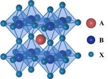
Figure 1. Schematic diagram of perovskite crystal structure.
The A-site cation, typically comprising organic methylammonium (MA⁺), formamidinium (FA⁺), or inorganic cesium (Cs⁺) ions, plays a crucial role in determining the lattice parameters and stability of the perovskite structure.[2,13,51] The ionic radius of the A-site cation directly influences the Goldschmidt tolerance factor (t), a key parameter governing structural stability.[40,52] When the tolerance factor approaches unity, the ideal cubic perovskite structure is favored. Larger A-site cations such as FA⁺ (2.79 Å) induce lattice expansion compared to MA⁺ (2.70 Å) or Cs⁺ (1.81 Å), leading to reduced B-X-B bond angles and consequent narrowing of the bandgap. This phenomenon explains why FAPbI₃ exhibits a smaller bandgap (1.48 eV) than MAPbI₃ (1.55 eV) or CsPbI₃ (1.73 eV). The dynamic nature of organic A-site cations also contributes to enhanced dielectric screening and defect tolerance in hybrid perovskites.[53,54]
At the B-site, divalent metal cations (Pb2+, Sn2+, or Ge2+) coordinate with halide anions to form the fundamental [BX6]4- octahedral units that constitute the electronic backbone of the material.[26,37,55] Lead-based perovskites dominate optoelectronic applications due to their superior stability and optoelectronic properties, but increasing attention has been paid to tin and germanium analogues for reduced toxicity.[9,13,56] The substitution of Pb²⁺ (1.19 Å) with larger Sn²⁺ (1.35 Å) increases the B-X bond length and decreases the bandgap, enabling near-infrared emission.[57] However, this comes at the cost of increased susceptibility to oxidation from Sn²⁺ to Sn⁴⁺.[57] The octahedral tilting induced by B-site substitution significantly affects carrier effective masses and exciton binding energies, with implications for charge transport and recombination dynamics.[58]
The X-site halide anions (Cl⁻, Br⁻, I⁻) provide perhaps the most straightforward route for bandgap engineering through compositional variation.[50] The bandgap of lead halide perovskites follows the trend MAPbCl₃ (3.11 eV) > MAPbBr₃ (2.30 eV) > MAPbI₃ (1.55 eV), reflecting the decreasing electronegativity and increasing orbital overlap from chloride to iodide.[9,14,22] Mixed-halide perovskites enable continuous bandgap tuning across the visible spectrum, though phase segregation under illumination remains a significant challenge for stable light emission.[50] The bond strength and polarizability of the halide anions also influence defect formation energies and non-radiative recombination pathways, with iodide perovskites generally exhibiting superior luminescence properties compared to their bromide and chloride counterparts.[59]
The structural versatility of perovskites extends beyond the classic 3D ABX₃ framework through dimensional engineering. By incorporating bulky organic cations such as phenethylammonium (PEA⁺) or butylammonium (BA⁺), the perovskite structure can be confined to two dimensions, forming quantum well structures with the general formula (A')₂(A)ₙ₋₁BₙX₃ₙ₊₁, where n represents the number of inorganic layers between organic spacers.[34,39,45,60] This dimensional reduction dramatically increases exciton binding energies from a few meV in 3D perovskites to hundreds of meV in quasi-2D perovskites, while also improving environmental stability through the hydrophobic organic layers.[26,61,62] The quantum confinement effects in low-dimensional perovskites offer additional knobs for property tuning through variation of the n-value distribution in quasi-2D systems.[33,63]
The structural stability and dimensionality of metal halide perovskites are fundamentally governed by the Goldschmidt tolerance factor (t) and the strategic incorporation of bulky organic cations.[31] The tolerance factor, defined as $t = (r_{A} + r_{B})/\sqrt{2(r_{B} + r_{X})}$, where rA, rB, and rX represent the ionic radii of the constituent ions, serves as a crucial predictor of perovskite formation and phase stability.[31] While the ideal cubic perovskite structure requires t ≈ 1, practical systems exhibit stability within the range of 0.81–1.0, with deviations from unity leading to symmetry-lowered structures such as tetragonal or orthorhombic phases.[29,64] This structural flexibility allows for significant compositional tuning while maintaining the essential perovskite framework, though extreme deviations may result in non-perovskite phases with compromised optoelectronic properties.
Dimensionality engineering has emerged as a powerful strategy to tailor the photophysical properties of perovskites, particularly through the development of quasi-2D systems.[33,41,60] These materials are characterized by the general formula (A′)2An-1BnX3n+1, where A′ represents a bulky organic cation (e.g., phenethylammonium or butylammonium) that spatially confines the inorganic [BX6]4- layers, and n denotes the number of inorganic sheets between organic spacers.[65,66] The introduction of these large organic cations breaks the continuous three-dimensional network of corner-sharing octahedra, creating natural quantum well structures with significantly enhanced exciton binding energies compared to their 3D counterparts.[67]
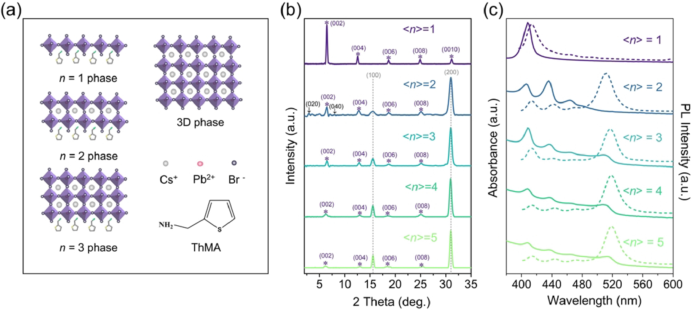
Figure 2. Structure (a) and XRD patterns (b) and absorptions/PL (c) of typical phase engineering perovskites (2-thiophenemethylammonium quasi-2D perovskites).[55]
A remarkable feature of quasi-2D perovskites is their inherent tendency to form mixed-phase systems with varying n-values during solution processing.[25,59,68] This heterogeneity, rather than being detrimental, enables an efficient energy funneling mechanism where photoexcited carriers rapidly transfer from higher-bandgap (low-n) phases to lower-bandgap (high-n) domains.[41,69] This process effectively concentrates excitons in the most stable, low-energy states, dramatically enhancing radiative recombination efficiency.[70] The energy transfer dynamics are particularly favorable for light-emitting applications, as the graded potential landscape minimizes non-radiative losses at interfaces and defects.[41,70] Moreover, the bulky organic cations provide a protective barrier against environmental degradation while maintaining efficient charge transport through the interconnected inorganic domains.[69]
At the extreme of dimensional reduction, zero-dimensional perovskite NCs represent another important class of materials with unique quantum confinement effects.[16] Typically synthesized through ligand-assisted reprecipitation or hot-injection methods, these nanostructures with sizes below 100 nm exhibit discrete electronic states and size-tunable optical properties.[12,29,71] The strong quantum confinement in these systems leads to enhanced oscillator strengths and narrow emission linewidths, making them particularly attractive for high-color-purity light-emitting applications.[16,43,72] Surface ligand engineering plays a critical role in NC stability and photoluminescence quantum yield, with appropriate passivation strategies capable of achieving near-unity emission efficiency.[12,31,73–75] The synthesis approaches allow precise control over nanocrystal size and shape, enabling further tuning of optoelectronic properties through morphological design.[73,74]
The dimensional control of perovskite materials offers a versatile platform for property engineering, with quasi-2D systems presenting particular advantages for light-emitting applications.[56] The combination of quantum confinement effects, efficient energy funneling mechanisms, and improved environmental stability makes these materials highly promising for next-generation optoelectronic devices. The ability to fine-tune the dimensionality through careful selection of organic spacers and processing conditions provides researchers with multiple degrees of freedom to optimize material performance for specific applications.
2.2 Luminescence Properties and Carrier Dynamics
The light-emitting properties of metal halide perovskites are governed by complex carrier dynamics that are highly sensitive to material composition, dimensionality, and excitation conditions.[21,56,76,77] Understanding these processes is crucial for optimizing light-emitting applications, as they determine the efficiency of radiative recombination and the nature of light emission - whether via exciton or free-carrier pathways.
2.2.1 Excitation and Recombination Pathways
The competition between exciton and free-carrier emission in perovskites is dominated by the exciton binding energy (Eb), which varies significantly with the halide composition and structural dimensionality.[78–80]
In 3D perovskites, dielectric screening effects reduce the Coulomb attraction between electrons and holes, resulting in relatively low exciton binding energies.[62] For example, MAPbI3 has an Eb of about 16 ± 2 meV at room temperature, which is comparable to the thermal energy (kBT ≈ 26 meV), which favors the dissociation of excitons into free carriers.[61] This free-carrier-dominated behavior is beneficial for photovoltaic applications but may limit the radiative efficiency of light-emitting devices due to nonradiative losses at defects and grain boundaries.[35] In contrast, bromide-based perovskites such as MAPbBr3 exhibit stronger exciton properties with Eb ranging from 67 to 150 meV, which is attributed to the higher electronegativity of Br⁻ and reduced dielectric screening.[13,35] This enhanced exciton stability makes bromide perovskites more suitable for efficient light emission.[13]
In quasi-2D and 2D perovskites, the situation changes dramatically, and the dielectric confinement effect caused by the alternating organic-inorganic layers drastically increases the exciton binding energy (>100 meV).[30,81] This strong confinement effect stabilizes excitons even at room temperature, suppresses non-radiative recombination and improves the photoluminescence quantum yield (PLQY).[58,82] The graded energy landscape in hybrid quasi-2D films further improves the emission efficiency by directing excitons to low-energy domains where radiative recombination dominates.[83]
2.2.2 Carrier Cooling and Dephasing Dynamics
Ultrafast carrier dynamics in perovskites play a crucial role in their luminescence properties.[78] After photoexcitation, hot carriers undergo rapid thermalization and cooling before recombination.[78] Notably, perovskites exhibit extremely long dephasing times (about 220 fs for MAPbI₃), significantly longer than conventional semiconductors such as GaAs (about 50 fs).[84,85] This extended coherence time is beneficial for population inversion, a key requirement for optical gain and laser applications.
Due to strong electron-phonon coupling, carrier cooling typically occurs in sub-picosecond timescales (about 100 fs).[76,86] However, at high excitation densities, a phonon bottleneck effect occurs, where the rapid accumulation of hot carriers saturates the available phonon modes, slowing down the cooling rate.[87,88] This effect is particularly pronounced in perovskite nanocrystals and two-dimensional systems, where quantum confinement enhances carrier-phonon interactions.[79] Delayed cooling enables efficient hot carrier extraction or radiative recombination before the energy is lost to thermal dissipation, which can be exploited in high-performance LEDs and lasers.[89]
2.2.3 Implications for Light-Emitting Applications
The interplay between excitons and free-carrier recombination, as well as the unique carrier cooling dynamics, determine the luminescence efficiency of perovskite-based devices.[56] Strategies such as halide alloying, size control, and surface passivation can be used to tune these dynamics—enhancing exciton stability in (quasi-) 2D systems or optimizing free-carrier transport in 3D analogs.[21,76,78] In addition, slow dephasing and phonon bottleneck effects indicate that perovskites are ideal candidates for ultrafast photonics and laser technologies, where long carrier coherence and controlled cooling paths are critical.[86]
Thus, by carefully designing the composition and structure, the luminescence properties of perovskites can be precisely tuned to meet the needs of next-generation optoelectronic devices.
2.2.4 Competition between radiative and non-radiative processes
The luminescence efficiency of perovskite materials fundamentally depends on the competition between radiative recombination and various non-radiative loss pathways, including defect-assisted Shockley-Read-Hall (SRH) recombination, Auger recombination, and surface/interface trapping.[4,11,90] The dominance of each process depends on the material composition, dimensionality, and excitation conditions, and therefore needs to be carefully designed to maximize the luminescence efficiency.[90]
Defect-assisted non-radiative recombination
In 3D perovskites, defects such as halide vacancies, interstitial ions, and anti-substitutions introduce mid-bandgap trap states, which promote non-radiative recombination and significantly reduce the photoluminescence quantum yield (PLQY) at low carrier density.[26] However, at high excitation levels, these traps saturate, resulting in the dominance of radiative interband transitions - a phenomenon known as the defect tolerance of perovskites.[62] This effect explains why 3D perovskite LEDs generally require high current density to reach peak efficiency.
Quasi-2D perovskites exhibit higher defect tolerance due to their mixed-phase nature.[69] The energy funneling mechanism preferentially directs excitons to regions with lower n values (larger band gaps), where trap density is typically lower. In addition, bulky organic ligands in 2D systems can passivate surface defects, further suppressing nonradiative losses.[41] Advanced phase engineering strategies, such as controlling the n value distribution through precursor stoichiometry or solvent treatment, can optimize this energy transfer process to achieve a PLQY close to 1 even at low excitation densities.[41]
Auger recombination and its dimensionality dependence
While defect-related losses can be mitigated, Auger recombination (a three-carrier interaction in which electron-hole pairs nonradiatively recombine by transferring energy to a third carrier) becomes a key limiting factor at high carrier densities.[74] This process is particularly severe in bromide-based perovskites and low-dimensional systems due to their larger exciton binding energies and stronger Coulomb interactions compared to iodide-based perovskites.[3,40] For example, the Auger coefficient of 2D perovskites (~10−28 cm6/s) is an order of magnitude higher than that of 3D perovskites, which poses a fundamental limitation on the optical gain threshold of lasers and high-brightness LEDs.[91]
However, quasi-2D perovskites have a unique advantage: the energy funneling mechanism spatially separates excitons, reducing their local density and thus suppressing Auger losses.[41] This explains why quasi-2D films can sustain ASE at a much lower threshold than 3D perovskites, making them ideal for low-threshold laser applications.
3. Engineering Approaches to Improve ASE Properties
Metal halide perovskite materials have attracted widespread attention in recent years for ASE and integrated laser applications due to their excellent optical gain properties, narrow emission bandwidths, and low excitation thresholds.[3,37,48,92,93] However, their ASE performance is influenced by multiple factors such as crystal quality, phase purity, defect-state density, and carrier dynamics, necessitating precise optimization through systematic engineering strategies.[15,37,51]
To address these challenges, researchers have developed a series of engineering approaches spanning multiple aspects—from material design, film fabrication processes, and microstructure control to device interface construction.[36,55] These strategies include phase engineering, solvent engineering, additive engineering, doping engineering, ligand engineering, structural engineering, and encapsulation/composite engineering. Such methods not only optimize energy level structures and carrier transport pathways and suppress non-radiative recombination but also significantly enhance material photostability and environmental tolerance. Through the synergistic effect of multiple strategies, the ASE threshold of perovskites is effectively reduced, while emission intensity and duration are substantially improved, laying an important foundation for the practical realization of high-performance, repeatedly excitable perovskite-based lasers in the future.
3.1. Phase Engineering
The distribution of layer numbers (n-value phases), phase purity, and compositional uniformity within quasi-2D perovskite materials critically influence their optical gain properties, especially ASE behavior.[55,58,94] Lower-n phases (e.g., n = 1, 2) exhibit strong exciton binding energies but act as deep energy traps that hinder efficient carrier transfer to higher-n domains, which are primarily responsible for radiative recombination.[75] This phase heterogeneity can elevate ASE thresholds and limit gain efficiency, while also reducing device stability and reproducibility.[30,34,60]
To address these challenges, phase engineering strategies focus on precise layer distribution control to suppress low-n phases and enrich high-n domains, thus optimizing the exciton population and enhancing radiative recombination rates. For example, Yao et al. demonstrated that tuning the phase composition towards n = 3 in PBA₂(MAPbBr₃)ₙ₋₁PbBr₄ films lowered the ASE threshold significantly from 29.91 to 19.23 mJ cm⁻², indicating an optimal balance between phase distribution and photophysical properties.[95]
Beyond layer tuning, enhancing phase purity through controlled crystallization and additive-assisted processing is essential. Wang et al. introduced adipic acid (AA) as an additive to regulate crystallization kinetics, achieving more homogeneous phase distributions, suppressed defect states, and a dramatic reduction in ASE threshold from 55.4 to 7.8 μJ cm⁻², along with a fourfold increase in gain coefficient.[24] Such improvements directly correlate phase uniformity with gain performance and device efficiency.
Moreover, composition optimization via humidity-controlled fabrication or organic additive incorporation further stabilizes the phase distribution. Zhang et al. utilized benzimidazole (BI) under ambient conditions to suppress multiphase separation, resulting in narrowed phase distribution and enhanced operational stability, as evidenced by a low ASE threshold of 13.4 μJ cm⁻² and a high number of half-decay pulses (5.6 × 10⁷).[40]
Collectively, these phase engineering strategies — spanning layer distribution control, phase purity enhancement, and compositional optimization — synergistically minimize non-radiative losses and improve exciton dynamics, thereby enabling low-threshold, high-efficiency ASE with enhanced stability. This comprehensive control over phase characteristics is thus fundamental to the advancement of high-performance, stable perovskite optoelectronic devices.
3.2. Solvent Engineering
Solvent composition and the crystallization environment critically influence the morphology, crystallinity, and phase distribution of quasi-2D perovskite films, thereby directly impacting their ASE performance.[38,39,96] Fine-tuning the solvent ratio, particularly of commonly used solvents such as dimethyl sulfoxide (DMSO) and dimethylformamide (DMF), effectively modulates the precursor coordination complexes and nucleation kinetics. This control over crystallization dynamics enables adjustment of grain size and film uniformity, both essential for minimizing nonradiative recombination and optimizing optical gain.
For example, Zhao et al. systematically investigated solvent evaporation effects during spin-coating, demonstrating that controlled evaporation rates substantially enhance film microstructure. The improved crystallinity resulted in a decreased ASE threshold down to 16.2 μJ cm⁻², accompanied by accelerated radiative biexciton recombination, which is beneficial for achieving efficient population inversion in lasing applications.[97]
In addition to solvent ratio optimization, the choice and application of antisolvents play a pivotal role in suppressing undesirable intermediate phases and promoting smooth, compact films. Wang et al. showed that using low-polarity antisolvent diisopropyl ether (DIE) effectively eliminated residual PbBr₂ intermediate phases, yielding films with ultrasmooth surfaces (RMS roughness ~1.82 nm) and prolonged carrier lifetimes (up to 1.24 ns). These improvements directly translated to a lower ASE threshold from 20.75 to 14.69 μJ cm⁻², highlighting the importance of antisolvent polarity and boiling point in phase control.[39]
Moreover, the crystallization atmosphere during film formation has emerged as another critical parameter. Zou et al. introduced a solvent atmosphere-assisted crystallization method utilizing DMSO vapor to retard surface crystallization. This approach promoted uniform phase distribution, reduced defect densities, and suppressed nonradiative recombination, achieving an exceptionally low ASE threshold of 12.9 μJ cm⁻² under pulsed optical excitation. Coupled with a microcavity structure, continuous-wave (CW) ASE at room temperature was realized with a threshold as low as 3.8 W cm⁻².[96]
In summary, solvent engineering—encompassing solvent composition tuning, antisolvent selection, and atmosphere-assisted crystallization—constitutes a versatile and effective strategy for optimizing quasi-2D perovskite film quality. This multidimensional control facilitates enhanced optical uniformity, reduced trap-assisted recombination, and improved ASE stability and repeatability, laying a solid foundation for the advancement of high-performance perovskite optoelectronic devices.
3.3. Additive Engineering
Additive engineering has emerged as a versatile and powerful strategy to enhance the ASE performance of perovskite materials by simultaneously tuning their crystallization behavior, defect landscape, and microstructural order. By incorporating functional molecules—such as long-chain alkylammonium salts, surfactants, and macrocyclic chelators—into the precursor solution, researchers have demonstrated multifaceted improvements in film morphology, phase purity, and optical gain properties.
One key function of additives is to modulate crystallization kinetics, promoting smoother film growth and suppressing defect-inducing pathways. For instance, the incorporation of long-chain octylammonium halide has been shown to facilitate the formation of highly compact, pinhole-free CsPbX₃ films with sub-2 nm surface roughness, significantly reducing light scattering and supporting low-threshold ASE operation.[98] Such additives help regulate the interaction between precursor species and substrate interfaces, thereby ensuring more uniform nucleation and phase distribution across the film.
In quasi-2D systems, simultaneous control of surface morphology and trap density is particularly critical. Surfactant-type additives such as Tween 80 have been employed not only to refine the film topography but also to passivate undercoordinated Pb²⁺ ions. This dual role has been correlated with a 10-fold suppression of nonradiative recombination and a substantial enhancement in optical gain, enabling ASE thresholds as low as 3.4 μJ cm⁻².[68] Such findings highlight the potential of soft amphiphilic additives to govern both film quality and exciton dynamics through interfacial interactions.
Another important application of additive engineering lies in phase composition regulation—especially promoting high-n phases in quasi-2D systems. Macrocyclic ligands such as 18-crown-6 ethers have been shown to selectively coordinate with A-site cations (e.g., FA⁺), subtly altering ionic equilibria during film formation. This strategy leads to smoother crystallization pathways and a favorable vertical alignment of perovskite layers, as evidenced by improved carrier cascade efficiency and reduced ASE threshold.[25] More importantly, when combined with high-quality feedback structures, such optimized films can even support continuous-wave (CW) lasing at room or cryogenic temperatures, underscoring the importance of structural and phase engineering at the molecular level.
Overall, additive engineering provides a highly modular platform for tailoring perovskite gain media. Through careful molecular selection, additives can simultaneously influence nucleation thermodynamics, suppress deep-level traps, and guide anisotropic growth. As demonstrated by multiple studies, the integration of additive-based strategies with other engineering approaches (e.g., phase and solvent control) will likely be central to the continued advancement of stable, low-threshold, and integrable perovskite lasers.
3.4. Doping Engineering
Doping engineering has emerged as an effective strategy to modulate the electronic structure, defect states, and phase behavior of quasi-2D perovskites, thereby substantially enhancing their ASE performance.[37,40] The incorporation of various cations—such as Rb⁺, K⁺, Mn²⁺, and Bi³⁺—into the perovskite lattice can lead to beneficial modifications in exciton binding energy, defect passivation, phase distribution, and charge carrier dynamics.
A representative example is provided by Tang et al., who investigated quasi-2D hybrid perovskites composed of mixed Dion–Jacobson (DJ) and Ruddlesden–Popper (RP) phases through structural modulation enabled by organic cation doping.[37] By adjusting the DJ/RP ratio, they achieved improved film morphology, phase uniformity, and gain characteristics. Specifically, the ASE threshold was reduced from 52.2 to 30.1 μJ cm⁻² and the gain coefficient was enhanced from 379 to 785 cm⁻¹. These improvements were attributed to enhanced crystallinity and better carrier transport induced by the DJ framework, highlighting the role of structural-phase doping in optimizing the ASE gain medium.
In another study, Guo et al. introduced K⁺ ions as dopants to control the crystallization kinetics of quasi-2D perovskites.[90] The electrostatic interaction between the alkali metal ions and [PbBr₆]⁴⁻ octahedra regulated nucleation pathways, leading to a more spatially homogeneous distribution of different-n phases. This spatial uniformity facilitated efficient energy funneling and reduced nonradiative losses, which are critical for population inversion. While this study was focused on LEDs, the underlying phase management principles and improved radiative efficiency are directly applicable to ASE systems as well.
Beyond intentional doping, even unintentional dopants can influence ASE behavior in perovskite systems. Ščajev et al. investigated CH₃NH₃SnI₃ films exhibiting spontaneous p-type doping due to processing conditions.[1] Surprisingly, despite structural imperfections, these Sn-based films showed remarkably low ASE thresholds (as low as 5 μJ cm⁻²) and high ambipolar carrier diffusion coefficients (up to 1.5 cm²/s under intense pumping). Their results suggest that moderate carrier self-doping may enhance stimulated emission processes by promoting carrier degeneracy and diffusion-driven population inversion, offering an unconventional route to boost gain performance.
Taken together, these studies underscore the pivotal role of doping engineering in modulating the photophysical properties of quasi-2D perovskite gain media. Whether through alkali metal-induced crystallization control, multivalent ion-mediated defect passivation, or structural-phase optimization via organic diammonium species, dopants serve as effective levers to regulate phase uniformity, exciton dynamics, and carrier transport pathways—all of which are intimately linked to ASE performance.[99–101] Importantly, these doping strategies not only enable reduced threshold fluences and enhanced optical gain, but also expand the materials’ compositional and dimensional versatility, paving the way toward robust and tunable perovskite laser platforms. As the field advances, the rational design of dopants—considering their ionic radius, charge state, coordination behavior, and interaction with the perovskite lattice—is expected to play an increasingly central role in achieving low-threshold, high-stability ASE operation across broader spectral regimes.
3.5. Ligand Engineering
Ligand engineering has emerged as a pivotal strategy to modulate surface states, defect passivation, and phase distribution in metal halide perovskite gain media.[31,74] The incorporation of functional organic ligands—such as alkylamines (e.g., octylamine), aromatic ammonium salts (e.g., phenylethylammonium, PEA), and phosphonate derivatives—enables selective coordination with undercoordinated metal cations or halide anions at specific crystallographic facets (e.g., {100}, {110}).[12,73,78] This coordination leads to the formation of stable, ordered organic capping layers that suppress trap-assisted nonradiative recombination and enhance surface energy alignment.[4,62] These effects are particularly critical for improving the stability and efficiency of ASE in perovskite-based photonic devices.
In quasi-2D perovskites, surface ligands not only reduce grain boundary defects but also play a structural role in guiding vertical crystal orientation. This vertical alignment favors anisotropic energy transport along the out-of-plane direction, forming efficient optical waveguides for ASE. For instance, phenylethylammonium (PEA) has been widely used to construct layered quasi-2D perovskites with high photoluminescence efficiency. However, Leyden et al. observed that excessive PEA content can introduce interfacial charge-transfer states that compete with the ASE process, leading to increased ASE thresholds and suppressed radiative recombination1. Their study emphasizes the necessity of balancing ligand quantity and dimensionality order to simultaneously optimize charge transport and exciton dynamics.[102]
Beyond excitonic control, ligands also offer environmental protection. Chen et al. demonstrated that long-chain alkylammonium ligands such as octylammonium (OA) significantly enhance the ambient stability of quasi-2D CsPbBr₃ films. The resulting OA-CsPbBr₃ films exhibited vertically aligned domains and hydrophobic surfaces that suppressed moisture penetration and maintained low ASE thresholds over 8 months of air storage without encapsulation.[36] This work highlights how structural and chemical synergy introduced by ligands can produce robust perovskite gain layers suitable for long-term optoelectronic operation.
Ligand passivation is equally vital in perovskite quantum dots (QDs), where surface defects and batch-to-batch variability often degrade ASE performance. To address this, Tao et al. employed a dual-ligand approach using acetate (AcO⁻) and 2-hexyldecanoic acid (2-HA) to simultaneously optimize cesium precursor reactivity and QD surface chemistry3. AcO⁻ improved precursor purity and yield, while 2-HA provided stronger coordination to passivate dangling surface bonds, effectively suppressing Auger recombination and enhancing ASE performance.[74] Their optimized CsPbBr₃ QDs exhibited a 70% reduction in ASE threshold (from 1.8 μJ·cm⁻² to 0.54 μJ·cm⁻²), near-unity PL quantum yield (99%), and excellent spectral uniformity, showcasing the power of tailored ligand chemistry.
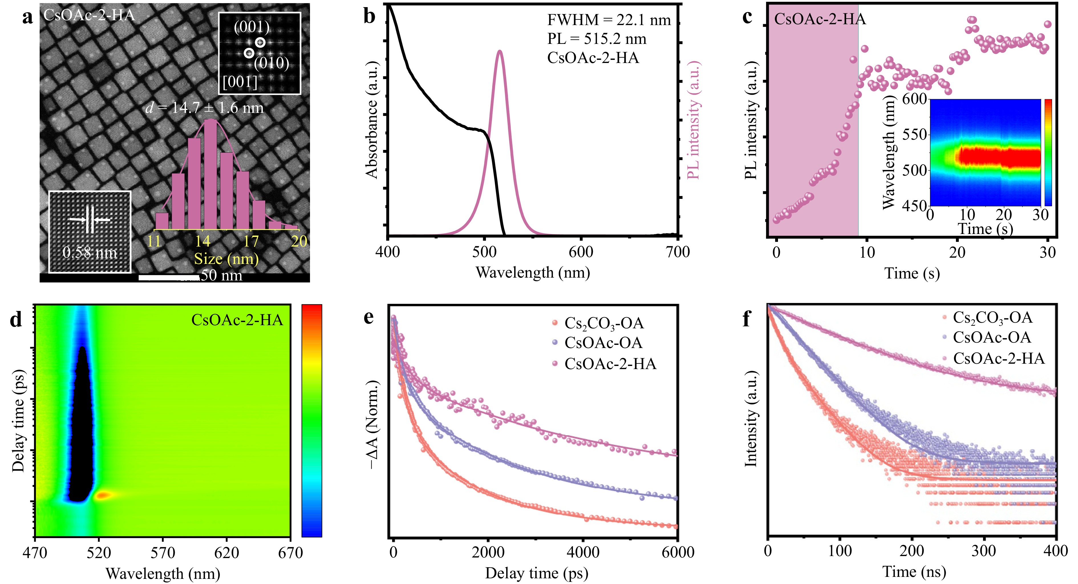
Figure 3. Optical properties of the perovskite CsPbBr3 QDs prepared with 2-HA: (a) TEM images, (b) UV–vis absorption and PL spectra, (c) in-situ PL spectra, (d) pseudo-color TA plot of CsOAc-2-HA QDs. Insets show the corresponding size distribution histograms, FFT, and IFFT images. (e) TA bleach recovery curves, and (f) time-resolved PL-decay transients of Cs2CO3-OA, CsOAc-OA, and CsOAc-2-HA QDs.[74]
In summary, ligand engineering operates at the intersection of structural control, excitonic modulation, and environmental stabilization. Through the judicious design of surface ligands and their interaction with the perovskite lattice, researchers can finely regulate optical gain properties, reduce ASE thresholds, and prolong operational lifetimes. This multifaceted role positions ligand engineering as a cornerstone in the development of high-performance, air-stable perovskite ASE platforms and next-generation coherent light sources.
3.6. Structural Engineering
The rational design of nanostructures and the employment of template-assisted methods have emerged as powerful strategies to enhance ASE performance in metal halide perovskite materials.[43,103] By tailoring the macroscopic film morphology, such as forming mesoporous frameworks, heterojunction interfaces, stacked multilayers, or photonic crystals, structural engineering can significantly improve optical gain and emission directionality.[4,104–106] These structural motifs often lead to stronger local electromagnetic fields, enhanced spatial confinement of excitons, and the construction of effective optical feedback cavities—key features for achieving low-threshold and high-intensity ASE.
Mesoporous perovskite structures, in particular, offer high surface-to-volume ratios and multiple scattering paths that can prolong the optical path length and amplify local light–matter interaction. For example, Soriano-Díaz et al. reported a MAPbBr₃–Ni(AcO)₂ nanocomposite waveguide structure wherein photon recycling between nanocrystals of different sizes significantly boosted the light amplification, achieving a remarkably low ASE threshold of ~1 µJ·cm⁻² and a high quality factor over 10⁴.[45] Such photon recycling within a guided geometry represents an efficient pathway to reduce the carrier density requirement for lasing while simultaneously narrowing the emission bandwidth.
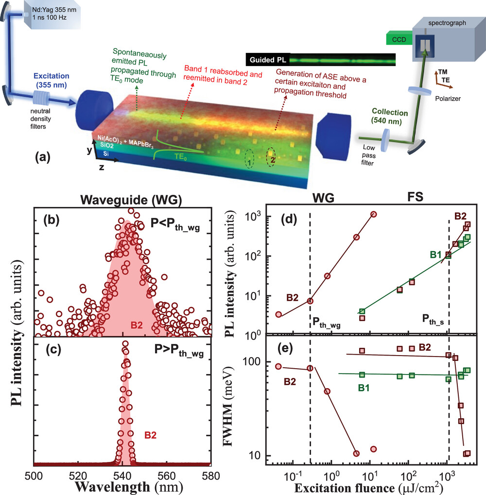
Figure 4. (a) Experimental set-up used to analyze the propagation of light/PL. Characterization of ASE in waveguide of 2 mm length: (b) below threshold, (c) above threshold. (d) Integrated PL and (e) FWHM of spectra deconvoluted from family 1 (green symbols) and family 2 (brown symbols) as a function of the excitation fluence. Circle and square symbols refer to the waveguide and transmittance geometries, respectively. Blue line, symbols, green area, and red area refer to the absorption spectra, experimental PL, emission from the B1, and emission from the B2, respectively.[45]
Another effective approach is to leverage plasmonic coupling and waveguiding effects through structural integration with metallic nanostructures. Xing et al. demonstrated a plasmonic-waveguide nanolaser composed of CsPbBr₃ quantum dots coupled with embedded silver nanowires (Ag NWs). The Ag NWs not only serve as a resonant cavity but also guide plasmonic modes that facilitate directional emission. When excitation was focused on individual NWs, a sub-nanometer full width at half maximum (FWHM) of 0.4 nm was achieved, highlighting the potential of structural hybridization for miniaturized on-chip coherent light sources.[42]
Beyond waveguide geometries, structural additives can play a crucial role in stabilizing film morphology under high-power operation. Azeem et al. introduced graphene oxide (GO) into quasi-2D perovskite films alongside Dion–Jacobson phase components to suppress thermal degradation and ensure structural coherence under extended heating at 130 °C. The optimized films preserved low ASE thresholds (21–25 mJ·cm⁻²) and sustained amplified emission under ambient annealing conditions, illustrating the synergistic stabilization enabled by structural modifiers.[60]
Taken together, these findings highlight the indispensable role of structural engineering in enabling robust and efficient ASE in perovskite systems. Whether by optimizing light–matter interaction pathways, promoting directional emission, or enhancing environmental resilience, structural design provides a versatile toolkit for the development of integrated, high-performance perovskite photonic devices.
3.7. Encapsulation/Composite Engineering
Due to the intrinsic ionic nature and soft lattice of metal halide perovskites, their optoelectronic performance—especially ASE—is highly susceptible to environmental stressors such as moisture, oxygen, UV irradiation, and thermal cycling.[36,107] These factors often accelerate structural degradation, induce non-radiative trap states, and suppress excited-state lifetimes, significantly limiting the optical gain and reproducibility of perovskite-based ASE systems.[73,106] Therefore, encapsulation and composite engineering have emerged as indispensable strategies for improving the operational stability and practical applicability of perovskite photonic devices.
A widely adopted approach involves physically embedding perovskite NCs or thin films into robust inorganic or polymer matrices, such as glass, PMMA, epoxy resin, or multilayer polymer barriers. These composite structures effectively isolate the active perovskite layer from environmental triggers while mitigating ion migration and phase instability. For instance, Zhang et al. synthesized core–shell FAPbBr₃/CsPbBr₃ nanocrystals, where the epitaxially grown CsPbBr₃ shell not only passivated surface defects but also suppressed ion migration, yielding a quasi-type II band alignment that sustained structural integrity and ASE activity under pulsed nanosecond excitation. The core–shell structure achieved an ASE threshold as low as 447 nJ·cm⁻², demonstrating the dual benefits of encapsulation and compositional modulation.[108]
Glass matrix embedding offers a more durable pathway to stabilization. He et al. reported Gd³⁺-doped CsPbCl₁.₅Br₁.₅ NCs embedded in borosilicate glass via melt-quenching and in-situ crystallization. The incorporation of Gd³⁺ enhanced thermal robustness and improved photoluminescence through defect passivation. These glass-embedded systems showed tunable ASE thresholds down to 0.39 mJ·cm⁻², depending on doping concentration and heat-treatment conditions.[109] Similarly, Zhang et al. demonstrated that glass network modulation via ZrO₂ additives promoted compact QD growth and suppressed Auger recombination, enabling a record-low ASE threshold of 54.5 μJ·cm⁻² and a modal gain coefficient exceeding 390 cm⁻¹ under femtosecond laser excitation. Notably, the glass-encapsulated CsPbBr₃ maintained quasi-continuous ASE even under prolonged exposure, outperforming colloidal systems by orders of magnitude in environmental stability.[110]
Further studies underscore the role of controlled crystallization in optimizing optical gain. Liu et al. encapsulated blue-emitting CsPbCl₂Br₁ NCs within borosilicate glass matrices using a thermally tuned precipitation method. The ASE threshold decreased dramatically from 1.24 to 0.19 mJ·cm⁻² as the heat-treatment temperature increased, indicating that precise crystallization control is pivotal for achieving high optical quality. The resulting perovskite–glass composites exhibited superior photostability and air resistance, offering a chemically inert, scalable, and integration-friendly platform for ASE lasers.[106]
Table 1. ASE properties of NCs and quasi-2D perovskite thin films
| Gain materials | Engineering strategies |
ASE threshold [µJ cm−2] |
Year | Ref. |
|---|---|---|---|---|
|
CsPbBr₃ (Quasi-2D) |
Additive Engineering | 14.9 | 2019 | [98] |
| Ligand Engineering | 13.7 | 2024 | [36] | |
| Structural Engineering | 21 | 2025 | [60] | |
|
CsPbBr₃ (NCs) |
Ligand Engineering | 0.54 | 2025 | [74] |
| Structural Engineering | 37.6 | 2021 | [42] | |
| Encapsulation/Composite Engineering | 54.5 | 2025 | [110] | |
|
FAPbBr₃ (Quasi-2D) |
Phase Engineering | 13.4 | 2024 | [24] |
| Solvent Engineering | 16.2 | 2024 | [97] | |
| Solvent Engineering | 12.9 | 2025 | [39] | |
| Solvent Engineering | 12.9 | 2023 | [96] | |
| Additive Engineering | 3.4 | 2023 | [68] | |
| Doping Engineering | 30.1 | 2023 | [1] | |
| MAPbBr₃ | Phase Engineering | 19.23 | 2021 | [95] |
| (Quasi-2D) | Structural Engineering | 1 | 2025 | [45] |
|
FAPbI₃ (Quasi-2D) |
Additive Engineering | 35.9 | 2023 | [25] |
|
MAPbI₃ (Quasi-2D) |
Ligand engineering | 1.6 | 2018 | [102] |
|
MASnBr₃ (Quasi-2D) |
Doping Engineering | 5 | 2019 | [37] |
|
PEA2(FA0.7Cs0.3)2Pb3Br10 (Quasi-2D) |
Phase Engineering | 70 | 2024 | [40] |
|
FAPbBr3/CsPbBr3 (NCs) |
Encapsulation/Composite Engineering | 0.447 | 2021 | [108] |
|
CsPbCl₁.₅Br₁.₅ (Quasi-2D) |
Encapsulation/Composite Engineering | 390 | 2021 | [109] |
In conclusion, encapsulation/composite engineering synergistically enhances both environmental stability and optical performance of perovskite materials through physical isolation, structural passivation, and defect suppression. These strategies are vital to transitioning perovskite ASE systems from laboratory demonstrations to practical, long-lifetime applications in integrated photonic circuits, wearable devices, and ambient-stable coherent light sources.
4. Optoelectronic Applications of Perovskite Light-Emitting
4.1 Low-Threshold and High-Quality Film Lasers
Recent advances in perovskite-based lasers have demonstrated remarkable progress in achieving low-threshold operation and high optical quality through innovative material engineering and device architectures. This section systematically reviews key developments in the field, focusing on the interplay between material properties, fabrication techniques, and device performance.
4.1.1 Material Engineering for Low-Threshold Operation
The foundation for low-threshold perovskite lasers lies in precise control of film morphology and crystallinity.[39] presents a breakthrough in fabricating ultrasmooth quasi-2D perovskite films through antisolvent engineering, where diisopropyl ether (DIE) was identified as the optimal antisolvent for eliminating intermediate phases. This approach yielded films with exceptional surface smoothness (RMS roughness of 1.82 nm) and reduced trap densities, as evidenced by prolonged carrier lifetimes (1.24 ns). The resulting films demonstrated a 29% reduction in ASE threshold (14.69 μJ cm-2) compared to conventional methods. These findings are complemented by Ref. [111], which achieved record-low ASE thresholds of ~2.23 μJ cm-2 in quasi-2D lead-bromide perovskites through optimized gain coefficients and suppressed Auger recombination. The study further demonstrated a distributed feedback (DFB) laser with an ultralow threshold of 0.69 μJ cm-2, highlighting the importance of optical field-gain medium coupling.
4.1.2 Quantum Dot-Based Laser Systems
All-inorganic perovskite quantum dots (QDs) have emerged as promising gain media due to their superior stability and optical properties. Ref. [16] reported a hybrid VCSEL structure incorporating CsPbBr3 QDs that achieved an ultralow lasing threshold of 0.39 μJ/cm2 while maintaining stable operation over 5 hours under ambient conditions. This work was extended in Ref. [112], where CsPbBr3 QDs were integrated into polymer optical fiber amplifiers, demonstrating gain coefficients of 232.2 cm-1 and achieving >20 dB optical gain in the 530-540 nm range. Ref. [27] introduced an electrically switchable gain mechanism in CsPbBr3 VCSELs, reducing the lasing threshold to 1.3 μJ cm-2 under nanosecond pumping through controlled ion migration.
4.1.3 Advanced Fabrication Techniques and Novel Architectures
Ref. [80] developed a seeds-assisted space-confined growth method for producing high-quality all-inorganic perovskite microcrystal arrays. This approach yielded submicron plates exhibiting ultralow-threshold (0.22 μJ cm-2) single-mode WGM lasing, representing a significant advancement toward on-chip photonic integration. In parallel, Ref. [113] demonstrated a monolithic perovskite thin-film VCSEL using CH3NH3PbI3 embedded in a custom GaN-based resonator, achieving single-mode operation with a threshold of 7.6 μJ cm-2 and spatially coherent Gaussian beams.
4.1.4 Continuous-Wave Operation and Stability
A critical milestone was achieved by Ref. [114], which reported the first stable room-temperature continuous-wave lasing in quasi-2D perovskite films. Through triplet management strategies and high-Q DFB cavities, the study overcame the longstanding challenge of "lasing death" under CW pumping. This work provided crucial insights into exciton dynamics, identifying singlet-triplet annihilation as a key mechanism limiting population inversion.
4.1.5 Progress Toward Electrically Pumped Lasers
The realization of electrically pumped perovskite lasers remains a critical challenge, but recent breakthroughs in electrically modulated gain have demonstrated promising pathways toward this goal. Ref. [63] conducted a comprehensive evaluation of low-dimensional perovskites for electrically driven lasers, benchmarking ASE/lasing thresholds against high-current-density LED performance. Their analysis projected that current densities of 4-10 kA/cm2 would be necessary to achieve lasing, highlighting the need for improved device architectures and material optimization.
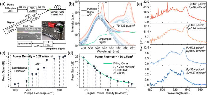
Figure 5. Optical gain measurement of Polymer optical fiber amplifier (POFA). (a) Experimental setup. The insets show the SEM image of the cross-sectional view of the POFA input facet and a photograph of POFA under 400-nm point source excitation. (b) Spectra of unpumped signal, pumped signals, and ASE with varying pump fluences. The inset shows a zoomed-in view of the optical gain region. (c) Peak optical gain vs pump fluences. (d) Peak optical gain vs signal power densities. (e) Gain spectra obtained at different pump fluences and signal power densities.[112]
A significant advancement was reported in Ref. [113], which demonstrated electric-field-enhanced ASE in CsPbBr3 perovskite LEDs. Unlike previous studies where electrical stimulation degraded optical gain, this work achieved a factor of 3 reduction in ASE threshold under a positive bias voltage. The enhancement was attributed to an electric-field-induced increase in radiative recombination rates, mediated by ion relocation on a ~10 s timescale. This finding provides the first experimental evidence that electrical biasing can actively lower lasing thresholds in perovskites, representing a crucial step toward overcoming the carrier injection bottleneck in future electrically pumped lasers.
4.2 Functional Expansion and Optoelectronic Synergy in Perovskite Lasers
Recent advances in perovskite lasers have transcended the conventional pursuit of low-threshold operation, evolving toward multifunctional integration and optoelectronic synergy. This section critically examines three pivotal breakthroughs that illuminate the intricate relationship between material engineering and device physics.
4.2.1 Speckle-Free Imaging with Quasi-2D Random Lasers
The inherent high spatial coherence of conventional lasers has long hindered their applications in high-resolution imaging due to speckle noise. Addressing this challenge, Ref. [30] demonstrated a breakthrough in quasi-2D (PEA)2MA3Pb4Br13 random lasers through adipic acid (AA) additive engineering. By modulating crystallization kinetics, the AA-modified films achieved exceptional phase uniformity while maintaining quantum-well-derived optical gain. The resultant random lasers exhibited a record-high gain coefficient of 1404 cm-1 and an 86% reduction in ASE threshold (7.8 μJ/cm2). Intriguingly, these devices preserved narrow emission bandwidth (<0.5 nm) while reducing spatial coherence by approximately 60% compared to conventional lasers—a unique combination enabling superior speckle-free imaging performance. Further analysis revealed that this performance stems from randomized phase information through multiple scattering, while the quantum-confined structures sustain sufficient gain for stimulated emission.
4.2.2 Defect-Tolerant ASE in Bulk Perovskite Crystals
Conventional wisdom suggests that quantum confinement is essential for efficient ASE. However, Ref. [115] challenged this paradigm by demonstrating ASE in millimeter-sized CsPbClxBr3-x crystals with substantial defect concentrations. At 50 K, these bulk crystals exhibited ASE at 456 nm with a threshold of 106 μJ/cm2. Temperature-dependent spectroscopic studies indicated that halogen vacancies facilitate the formation of localized excitons, which enhance radiative recombination at cryogenic temperatures. Remarkably, metal-semiconductor-metal (MSM) photodetectors fabricated from the same crystals showed rapid response times (96 μs rise time), suggesting minimal defect interference with carrier transport. This defect tolerance opens new possibilities for monolithically integrated devices combining laser emission and photodetection functionalities.
4.2.3 Layer-Dependent Optoelectronic Trade-offs
The systematic investigation of PBA2(MAPbBr3)n-1PbBr4 perovskites in Ref. [95] unveiled a nonlinear relationship between quantum-well number (n) and device performance. While the n=7 variant exhibited optimal photoluminescence characteristics (32 ns radiative lifetime at room temperature) due to balanced dielectric confinement and exciton binding energy, the lowest ASE threshold (19.23 μJ/cm2) occurred at n=3. This counterintuitive observation may arise from enhanced exciton-photon coupling in lower-dimensional structures. Contrastingly, 3D perovskites (n=∞) outperformed their quasi-2D counterparts in photocurrent generation under strong illumination, highlighting a fundamental trade-off between lasing efficiency and charge transport. These findings provide critical guidelines for application-specific material design, where dimensional engineering can tailor performance for either ultralow-threshold lasers or high-responsivity photodetectors.
5. Conclusions and Future Perspectives
5.1. Conclusion
This review systematically reviews the recent progress of perovskite lasers, focusing on their evolution from fundamental optoelectronic research to functional devices with customizable performance. Key breakthroughs include the development of quasi-two-dimensional random lasers for speckle-free imaging, the discovery of defect-mediated amplified spontaneous emission in bulk perovskite crystals, and the confirmation of a dimensionality-dependent trade-off between optical gain and charge transport. Together, these advances highlight the unique advantages of perovskites—tunable band gaps, high defect tolerance, and compatibility with low-cost manufacturing—that make them widely applicable in photonic applications.
A key insight from these studies is the delicate balance between material design and device performance. For example, while low-dimensional perovskites exhibit excellent lasing thresholds due to enhanced exciton confinement, their charge transport properties are often compromised, limiting their use in integrated optoelectronic systems. In contrast, bulk perovskites, despite their high defect density, have shown unexpected potential for fabricating dual-functional devices that combine lasing and photodetection. These findings challenge conventional design paradigms and open new avenues for multifunctional photonic platforms.
5.2. Future Perspectives
Looking ahead, several transformative opportunities and challenges remain to be addressed. First, achieving room temperature continuous wave operation in perovskite lasers is essential for practical applications. While low-temperature studies have provided valuable insights into carrier recombination dynamics, extending these principles to room temperature requires innovative approaches in materials engineering, such as strain modulation or advanced passivation techniques.
Second, the integration of perovskite lasers with existing photonic and electronic architectures, from silicon photonics to flexible substrates, is both a challenge and an opportunity. Developing scalable fabrication methods that ensure uniformity over large areas while maintaining optical performance is critical. Hybrid integration strategies, such as combining perovskites with plasmonic nanostructures or two-dimensional materials, can further enhance device functionality.
Finally, there is still much room for exploring perovskite lasers in emerging applications, such as quantum light sources, ultrafast optical switches, or bio-integrated sensors. Tunable emission wavelengths, ultrahigh brightness, and the potential for on-chip integration make perovskites a unique choice for next-generation photonic systems. However, realizing these applications requires interdisciplinary collaboration to address fundamental issues such as material stability, device reliability, and system-level optimization.
In summary, perovskite lasers are at a critical juncture where fundamental research is beginning to translate into functional technology. By addressing the challenges outlined in this article and leveraging the material’s inherent advantages, the field may soon see widespread use of perovskite-based light sources in science and industry.
Acknowledgements
This work was supported by the Shandong Provincial Natural Science Foundation (Grant ZR2024LZH008) and Shandong Province Scientific and Technological Achievement Transfer and Transformation Subsidy (Shandong-Chongqing Science and Technology Cooperation) Project.
References
-
Y. Tang, J. Guo, B. Liu, L. Qin, Z. Deng, Y. Hu, F. Teng, Z. Lou, Y. Hou. "Amplified spontaneous emission from waveguides based on hybrid quasi-2D perovskites of Dion–Jacobson and Ruddlesden–Popper phases." J. Mater. Chem. C 2023, 11, 29, 10043–50.
-
G. Xing, N. Mathews, S. S. Lim, N. Yantara, X. Liu, D. Sabba, M. Grätzel, S. Mhaisalkar, T. C. Sum. "Low-temperature solution-processed wavelength-tunable perovskites for lasing." Nat. Mater. 2014, 13, 5, 476–80.
-
G. Weng, J. Xue, J. Tian, X. Hu, X. Bao, H. Lin, S. Chen, Z. Zhu, J. Chu. "Picosecond Random Lasing Based on Three-Photon Absorption in Organometallic Halide CH3NH3PbBr3 Perovskite Thin Films." ACS Photonics 2018, 5, 7, 2951–59.
-
M. Athanasiou, P. Papagiorgis, A. Manoli, C. Bernasconi, M. I. Bodnarchuk, M. V. Kovalenko, G. Itskos. "Efficient Amplified Spontaneous Emission from Solution-Processed CsPbBr3 Nanocrystal Microcavities under Continuous Wave Excitation." Adv. Opt. Mater. 2021, 8, 7, 2120–29.
-
Y. Xiong, B. Chen, X. Xu, S. Dai, Y. Zhan, X. Xu. "Facile Fabrication of Highly Crystallized, Air‐Stable, and Flexible Perovskite Micromesh Film Photodetector." Adv. Opt. Mater. 2024, 12, 34, 2401287.
-
Y. Lei, Y. Chen, R. Zhang, Y. Li, Q. Yan, S. Lee, Y. Yu, H. Tsai, W. Choi, K. Wang, Y. Luo, Y. Gu, X. Zheng, C. Wang, C. Wang, H. Hu, Y. Li, B. Qi, M. Lin, Z. Zhang, S. A. Dayeh, M. Pharr, D. P. Fenning, Y.-H. Lo, J. Luo, K. Yang, J. Yoo, W. Nie, S. Xu. "A fabrication process for flexible single-crystal perovskite devices." Nature 2020, 583, 7818, 790–95.
-
M. Abdi-Jalebi, Z. Andaji-Garmaroudi, S. Cacovich, C. Stavrakas, B. Philippe, J. M. Richter, M. Alsari, E. P. Booker, E. M. Hutter, A. J. Pearson, S. Lilliu, T. J. Savenije, H. Rensmo, G. Divitini, C. Ducati, R. H. Friend, S. D. Stranks. "Maximizing and stabilizing luminescence from halide perovskites with potassium passivation." Nature 2018, 555, 7697, 497–501.
-
S. Yakunin, L. Protesescu, F. Krieg, M. I. Bodnarchuk, G. Nedelcu, M. Humer, G. De Luca, M. Fiebig, W. Heiss, M. V. Kovalenko. "Low-threshold amplified spontaneous emission and lasing from colloidal nanocrystals of caesium lead halide perovskites." Nat. Commun. 2015, 6, 1, 8056.
-
L. N. Quan, Y. Zhao, F. P. García De Arquer, R. Sabatini, G. Walters, O. Voznyy, R. Comin, Y. Li, J. Z. Fan, H. Tan, J. Pan, M. Yuan, O. M. Bakr, Z. Lu, D. H. Kim, E. H. Sargent. "Tailoring the Energy Landscape in Quasi-2D Halide Perovskites Enables Efficient Green-Light Emission." Nano Lett. 2017, 17, 6, 3701–09.
-
A. Balena, A. Perulli, M. Fernandez, M. L. De Giorgi, G. Nedelcu, M. V. Kovalenko, M. Anni. "Temperature Dependence of the Amplified Spontaneous Emission from CsPbBr3 Nanocrystal Thin Films." J. Phys. Chem. C 2018, 122, 10, 5813–19.
-
P. Papagiorgis, A. Manoli, L. Protesescu, C. Achilleos, M. Violaris, K. Nicolaides, T. Trypiniotis, M. I. Bodnarchuk, M. V. Kovalenko, A. Othonos, G. Itskos. "Efficient Optical Amplification in the Nanosecond Regime from Formamidinium Lead Iodide Nanocrystals." Adv. Opt. Mater. 2018, 5, 3, 907–17.
-
Z. Liu, Z. Hu, Z. Zhang, J. Du, J. Yang, X. Tang, W. Liu, Y. Leng. "Two-Photon Pumped Amplified Spontaneous Emission and Lasing from Formamidinium Lead Bromine Nanocrystals." ACS Photonics 2019, 6, 12, 3150–58.
-
M. S. Alias, I. Dursun, D. Shi, M. I. Saidaminov, E. M. Diallo, D. Priante, T. K. Ng, O. M. Bakr, B. S. Ooi. "Focused-ion beam patterning of organolead trihalide perovskite for subwavelength grating nanophotonic applications." Appl. Phys. Lett. 2015, 106, 5, 051102.
-
M. Li, Q. Gao, P. Liu, Q. Liao, H. Zhang, J. Yao, W. Hu, Y. Wu, H. Fu. "Amplified Spontaneous Emission Based on 2D Ruddlesden–Popper Perovskites." Adv. Funct. Mater. 2018, 28, 17, 1707006.
-
A. J. Wildenborg, R. J. Munter, F. Freire-Fernández, E. T. F. Freitas, J. Y. Suh. "Superlattice-Induced Superfluorescence in Quasi-2D Metal Halide Perovskites." Adv. Mater. 2025, 37, 1, 2304123.
-
C.-Y. Huang, C. Zou, C. Mao, K. L. Corp, Y.-C. Yao, Y.-J. Lee, C. W. Schlenker, A. K. Y. Jen, L. Y. Lin. "CsPbBr3 Perovskite Quantum Dot Vertical Cavity Lasers with Low Threshold and High Stability." ACS Nano 2017, 11, 9, 9259–67.
-
T. Erdem, H. V. Demir. "Colloidal nanocrystals for quality lighting and displays: milestones and recent developments." Nanophotonics 2016, 5, 1, 74–95.
-
J. W. Lim, H. Wang, C. H. Choi, H. Kwon, L. N. Quan, W.-T. Park, Y.-Y. Noh, D. H. Kim. "Self-powered reduced-dimensionality perovskite photodiodes with controlled crystalline phase and improved stability." Nano Energy 2019, 57, 761–70.
-
C. Shen, S. Fang, J. Zhang, X. Liang, C. Su, J. Qing, W. Cai, Y. Luo, R. Yang, L. Hou. "High performance and stable pure-blue quasi-2D perovskite light-emitting diodes by multifunctional zwitterionic passivation engineering." Adv. Photonics 2024, 6, 2, 026002.
-
Y. Wang, X. Li, V. Nalla, H. Zeng, H. Sun. "Solution‐Processed Low Threshold Vertical Cavity Surface Emitting Lasers from All‐Inorganic Perovskite Nanocrystals." Adv. Funct. Mater. 2017, 27, 13, 1605088.
-
M. Pelton. "Carrier Dynamics, Optical Gain, and Lasing with Colloidal Quantum Wells." J. Phys. Chem. C 2018, 122, 20, 10659–74.
-
M. Li, Q. Wei, S. K. Muduli, N. Yantara, Q. Xu, N. Mathews, S. G. Mhaisalkar, G. Xing, T. C. Sum. "Enhanced Exciton and Photon Confinement in Ruddlesden–Popper Perovskite Microplatelets for Highly Stable Low‐Threshold Polarized Lasing." Adv. Mater. 2018, 30, 23, 1707237.
-
D. Litvinas, R. Aleksiejūnas, P. Ščajev, P. Baronas, V. Soriūtė, C. Qin, T. Fujihara, T. Matsushima, C. Adachi, S. Juršėnas. "Energy transfer in (PEA)2FAn−1PbnBr3n+1 quasi-2D perovskites." J. Mater. Chem. C 2021, 9, 14, 4782–91.
-
X. Zhang, Y. Li, G. He, L. Xia, X. Qiao, D. Zhang, D. Yang, J. Chen, D. Ma, J. Peng. "Quasi‐CW Amplified Spontaneous Emission in Air‐Processed Quasi‐2D Perovskite Thin Films with High Stability." Adv. Opt. Mater. 2024, 12, 5, 2301876.
-
L. Gu, M. Li, J. Lai, D. Qian, K. Wen, L. Xu, G. Wang, S. Guan, Y. Zhang, X. Huang, J. Zhao, G. Xing, N. Wang, L. Zhu, Q. Peng, W. Huang, J. Wang. "High Q‐Factor and Low Threshold Continuous‐Wave Near‐Infrared Lasing with Quasi‐2D Perovskites." Adv. Funct. Mater. 2023, 33, 44, 2304123.
-
I. Allegro, Y. Li, B. S. Richards, U. W. Paetzold, U. Lemmer, I. A. Howard. "Bimolecular and Auger Recombination in Phase-Stable Perovskite Thin Films from Cryogenic to Room Temperature and Their Effect on the Amplified Spontaneous Emission Threshold." ACS Photonics 2021, 8, 7, 2104–12.
-
Y. Li, S. Liu, T. Feeney, J. Roger, M. Gholipoor, H. Hu, D. Zhao, I. Howard, F. Deschler, U. Lemmer, U. W. Paetzold. "Electrically‐Switchable Gain in Optically Pumped CsPbBr3 Lasers With Low Threshold at Nanosecond Pumping." Adv. Sci. 2025, 21, 13, 2401325.
-
Z. Yang, Y. Wu, N. Yang, R. Yang, Y. Hao. "Revealing the Role of Polyacrylonitrile for Highly Efficient and Stable Perovskite Solar Cells at Extremely Low Temperatures." Adv. Energy Mater. 2024, 14, 31, 2400638.
-
A. P. Pushkarev, V. I. Korolev, D. I. Markina, F. E. Komissarenko, A. Naujokaitis, A. Drabavičius, V. Pakštas, M. Franckevičius, S. A. Khubezhov, D. A. Sannikov, A. V. Zasedatelev, P. G. Lagoudakis, A. A. Zakhidov, S. V. Makarov. "A Few-Minute Synthesis of CsPbBr3 Nanolasers with a High Quality Factor by Spraying at Ambient Conditions." ACS Appl. Mater. Interfaces 2019, 11, 1, 1040–48.
-
J. Wang, J. Qin, Z. Zhan, Z. Hu, S. Huang, F. Zhou, Q. Li, Z. Liu, Z. Zhang, Y. Leng, J. Du. "Speckle-Free Imaging Based on a Quasi-2D Perovskite Random Laser with a Subwavelength Thickness." Adv. Opt. Mater. 2024, 11, 4, 1664–72.
-
A. Manoli, P. Papagiorgis, M. Sergides, C. Bernasconi, M. Athanasiou, S. Pozov, S. A. Choulis, M. I. Bodnarchuk, M. V. Kovalenko, A. Othonos, G. Itskos. "Surface Functionalization of CsPbBr3 Νanocrystals for Photonic Applications." ACS Appl. Nano Mater. 2021, 4, 5, 5084–97.
-
S. Milanese, M. L. De Giorgi, M. Anni, M. I. Bodnarchuk, L. Cerdán. "Rationalizing the Amplified Spontaneous Emission Mechanism in CsPbBr3 Perovskite Nanocrystals Films by means of Optical Gain Measurements." Nat. Commun. 2024, 15, 27, 3210.
-
G. Jin, T. Liu, Y. Li, J. Zhou, D. Zhang, P. Pang, Z. Ye, Z. Xing, G. Xing, J. Chen, D. Ma. "Low-dimensional phase suppression and defect passivation of quasi-2D perovskites for efficient electroluminescence and low-threshold amplified spontaneous emission." Nat. Photonics 2022, 16, 3, 919–29.
-
Y. Zhang, Z. Dong, X. Guo, Y. Hu, Z. Zhang, Y. Deng, Y. Zhang, Z. Men, C. Geng, Y. Wang, Z. Chen, Y. Jiang, L. Song, Y. Xia. "Enhanced performance of amplified spontaneous emission in Dion-Jacobson phase quasi-2D perovskite by facilitating carrier co-radiation." Opt. Express 2024, 32, 15, 26306.
-
M. W. Heindl, M. F. Lichtenegger, T. Kodalle, S. Liu, N. Solhtalab, J. Zerhoch, A. Shcherbakov, M. Kivala, C. M. Sutter‐Fella, A. S. Urban, F. Deschler. "Ligand‐induced crystallization control in MAPbBr3 hybrid perovskites for high quality nanostructured films." Adv. Opt. Mater. 2025, 13, 6, 2402441.
-
X. Chen, J. Qin, X. Wang, Y. Shu, M. Li, P. Zhou, G. Lu, H. He. "Long-term air-stable amplified spontaneous emission in quasi-2D perovskite films through ligand engineering." J. Mater. Chem. C 2024, 12, 22, 8119-26.
-
P. Ščajev, R. Aleksieju̅nas, P. Baronas, D. Litvinas, M. Kolenda, C. Qin, T. Fujihara, T. Matsushima, C. Adachi, S. Juršėnas. "Carrier Recombination and Diffusion in Wet-Cast Tin Iodide Perovskite Layers Under High Intensity Photoexcitation." J. Phys. Chem. C 2019, 123, 32, 19275-81.
-
Y. Liang, Q. Shang, M. Li, S. Zhang, X. Liu, Q. Zhang. "Solvent recrystallization‐enabled green amplified spontaneous emissions with an ultra‐low threshold from pinhole‐free perovskite films." Adv. Funct. Mater. 2021, 31, 48.
-
Y. Wang, W. Zhao, K. Zheng, C. J. S. Ponseca, Y. Cui, G. Li. "Formation of intermediate-phase free ultrasmooth quasi-two-dimensional perovskite films for high quality lasers." J. Mater. Chem. C 2025, 13, 24, 12341-47.
-
X. Wei, Z. Liu, J. Yang, X. Tang, Y. Wang, Y. Huang, Y. Yao, X. Xu, M. Pi, J. Du, D. Zhang. "Phase distribution management in quasi-2D perovskite films toward highly efficient amplified spontaneous emission pumped by nanosecond pulsed laser." Sci. China Mater. 2024, 67, 3, 921-30.
-
S. Huang, N. Liu, Z. Liu, Z. Zhan, Z. Hu, Z. Du, Z. Zhang, J. Luo, J. Du, J. Tang, Y. Leng. "Enhanced Amplified Spontaneous Emission in Quasi-2D Perovskite by Facilitating Energy Transfer." ACS Appl. Mater. Interfaces 2022, 14, 29, 33842-49.
-
D. Xing, C.-C. Lin, P. Won, R. Xiang, T.-P. Chen, A. S. A. Kamal, Y.-C. Lee, Y.-L. Ho, S. Maruyama, S. H. Ko, C.-W. Chen, J.-J. Delaunay. "Metallic nanowire coupled CsPbBr3 quantum dots plasmonic nanolaser." Adv, Funct, Mater, 2021, 31, 28, 2102375.
-
H. Xiao, Z. Liu, Q. Qian, J. Du, R. Li, Z. Zang. "Enhanced amplified spontaneous emission of CsPbBr3 quantum dots via gold nanorods-induced localized surface plasmon resonance." Appl. Phys. Lett. 2022, 121, 22, 222102.
-
L. Ye, S. Hong, Z. Zhang, Q. Zhao. "Enhanced random lasing from perovskite quantum dot with PMMA and LSPR of Ag nanoislands." Plasmonics 2025.
-
S. Soriano‐Díaz, J. Noguera‐Gómez, J. P. Martínez‐Pastor, P. P. Boix, R. Abargues, I. Suárez. "Photon recycling triggered amplified spontaneous emission in MAPbBr3‐Ni(AcO)2 nanocomposite waveguides." Laser Photonics Rev. 2025, 19, 10, 2401920.
-
X. Wu, Y. Li, W. Li, L. Wu, B. Fu, W. Wang, G. Liu, D. Zhang, J. Zhao, P. Chen. "Enhancing optically pumped organic-inorganic hybrid perovskite amplified spontaneous emission via compound surface plasmon resonance." Crystals 2018, 8, 3, 124.
-
Q. Mo, T. Shi, W. Cai, S. Zhao, D. Yan, J. Du, Z. Zang. "Room temperature synthesis of stable silica-coated CsPbBr3 quantum dots for amplified spontaneous emission." Photon. Res. 2020, 8, 10, 1605.
-
S. Chin, D. Cortecchia, M. Forzatti, C. Wu, A. L. Alvarado‐Leaños, G. Folpini, A. Treglia, I. A. Kalluvila Justin, A. Paliwal, C. Cho, C. Roldán‐Carmona, M. Sessolo, A. Petrozza, H. J. Bolink. "Stabilizing single‐source evaporated perovskites with organic interlayers for amplified spontaneous emission." Adv. Opt. Mater. 2024, 12, 13, 2302701.
-
K. Wu, A. Bera, C. Ma, Y. Du, Y. Yang, L. Li, T. Wu. "Temperature-dependent excitonic photoluminescence of hybrid organometal halide perovskite films." Phys. Chem. Chem. Phys. 2014, 16, 41, 22476-81.
-
S. M. H. Qaid, H. M. Ghaithan, B. A. Al-Asbahi, A. S. Aldwayyan. "Tuning of Amplified Spontaneous Emission Wavelength for Green and Blue Light Emission through the Tunable Composition of CsPb(Br1-xClx)3 Inorganic Perovskite Quantum Dots." J. Phys. Chem. C 2021, 125, 17, 9441-52.
-
X. Zhu, Y. Xie, X. Ma. "Achieving up-conversion amplified spontaneous emission through spin alignment between coherent light-emitting excitons in perovskite microstructures." Photonics 2022, 9, 5, 353.
-
Y. Li, I. Allegro, M. Kaiser, A. J. Malla, B. S. Richards, U. Lemmer, U. W. Paetzold, I. A. Howard. "Exciton versus free carrier emission: implications for photoluminescence efficiency and amplified spontaneous emission thresholds in quasi-2D and 3D perovskites." Mater. Today 2021, 49, 35-47.
-
L. Zhuang, C. Li, Q. Wei, R. Zhu, H. Ren, F. Shi, K. Leng, M. Li, S. Ye, S. P. Lau. "Harnessing Conformational Disorder of Organic Cations for Efficient Blue Quasi-2D Perovskite LEDs." Advanced Optical Materials 2024, 12, 14, 2302926.
-
J. Song, G. Zhou, W. Chen, Q. Zhang, J. Ali, Q. Hu, J. Wang, C. Wang, W. Feng, A. B. Djurišić, H. Zhu, Y. Zhang, T. Russell, F. Liu. "Unraveling the crystallization kinetics of 2D perovskites with sandwich‐type structure for high‐performance photovoltaics." Adv. Mater. 2020, 32, 36, 2002784.
-
C. Qin, S. Zhang, Z. Zhou, T. Han, J. Song, S. Ma, G. Jia, Z. Jiao, Z. Zhu, X. Chen, Y. Jiang. "Low amplified spontaneous emission threshold from 2-thiophenemethylammonium quasi-2D perovskites via phase engineering." Opt. Express 2022, 30, 20, 36541.
-
M. Cui, C. Qin, Y. Jiang, M. Yuan, L. Xu, D. Song, Y. Jiang, Y. Liu. "Direct Observation of Competition between Amplified Spontaneous Emission and Auger Recombination in Quasi-Two-Dimensional Perovskites." J. Phys. Chem. Lett. 2020, 11, 14, 5734–40.
-
P. Pang, G. Jin, C. Liang, B. Wang, W. Xiang, D. Zhang, J. Xu, W. Hong, Z. Xiao, L. Wang, G. Xing, J. Chen, D. Ma. "Rearranging Low-Dimensional Phase Distribution of Quasi-2D Perovskites for Efficient Sky-Blue Perovskite Light-Emitting Diodes." ACS Nano 2020, 14, 9, 11420–30.
-
A. Yu, J. Wang, Y. Huo, S. Wang, X. Zhang, T. He, S. Yang, Y. Jiang, L. Zhang, Z. Liu, M. Yuan, C. Sun. "Promoting Phase Transition in Quasi‐2D Perovskites For High‐Performance Pure‐Red LEDs." Advanced Materials 2025, 2503704.
-
G. Lu, Z. Chen, Z. Fang, H. Li, Y. Gao, C. Lin, X. Dai, Z. Ye, H. He. "Mixed Halide Perovskite Films by Vapor Anion Exchange for Spectrally Stable Blue Stimulated Emission." 2021, 17, 39.
-
A. Azeem, X. Wang, B. Hassan, M. Zhu, X. Dai, Z. Ye, Z. Chen, H. He. "Graphene oxide-enhanced mixed-structure quasi-2D perovskites for stable low-threshold amplified spontaneous emission." J. Mater. Chem. C 2025, 13, 27, 13847–55.
-
S. M. H. Qaid, A. S. Aldwayyan. "Aprotic Solvent Effect in Preparation of Organo Lead Iodide Perovskite Nanowires by Two-Step Spin-Coating Procedure." ECS J. Solid State Sci. Technol. 2023, 12, 2, 026004.
-
A. D. Sinelnik, E. V. Bodyago, O. M. Kushchenko, I. I. Shishkin, N. K. Kuzmenko, D. S. Gets, S. V. Makarov. "Three-dimensional perovskite-based photonic structures made by two-step crystallization." Opt. Laser Technol. 2024, 171, 110411.
-
M. R. Leyden, S. Terakawa, T. Matsushima, S. Ruan, K. Goushi, M. Auffray, A. S. D. Sandanayaka, C. Qin, F. Bencheikh, C. Adachi. "Distributed feedback lasers and light-emitting diodes using 1-naphthylmethylamnonium low-dimensional perovskite." ACS Photonics 2019, 6, 2, 460–66.
-
A. A. Lohar, A. Shinde, R. Gahlaut, A. Sagdeo, S. Mahamuni. "Enhanced Photoluminescence and Stimulated Emission in CsPbCl3 Nanocrystals at Low Temperature." J. Phys. Chem. C 2018, 122, 43, 25014–20.
-
J. Hu, I. W. H. Oswald, S. J. Stuard, M. M. Nahid, N. Zhou, O. F. Williams, Z. Guo, L. Yan, H. Hu, Z. Chen, X. Xiao, Y. Lin, Z. Yang, J. Huang, A. M. Moran, H. Ade, J. R. Neilson, W. You. "Synthetic control over orientational degeneracy of spacer cations enhances solar cell efficiency in two-dimensional perovskites." Nat Commun 2019, 10, 1, 1276.
-
S. Zeng, S. Shi, S. Wang, Y. Xiao. "Mixed-ligand engineering of quasi-2D perovskites for efficient sky-blue light-emitting diodes." J. Mater. Chem. C 2020, 8, 4, 1319–25.
-
S. Ghimire, L. Chouhan, Y. Takano, K. Takahashi, T. Nakamura, K. Yuyama, V. Biju. "Amplified and Multicolor Emission from Films and Interfacial Layers of Lead Halide Perovskite Nanocrystals." ACS Energy Lett. 2019, 4, 1, 133–41.
-
D. Zou, X. Guo, Z. Bao, Y. Lv, T. Wang, B. Zhang, X. Liu. "Low-Threshold Amplified Spontaneous Emission from Defect-Passivated Quasi-2D Perovskites." J. Phys. Chem. C 2023, 127, 44, 21841–48.
-
C. Zhao, C. Qin. "Quasi-2D lead halide perovskite gain materials toward electrical pumping laser." Nanophotonics 2021, 10, 8, 2167–80.
-
I. Wagner, W. T. M. Van Gompel, R. Erkens, B. Ruttens, J. D’Haen, L. Lutsen, D. Vanderzande, C. Chuang, S. H. Chang, P. A. Hume, M. B. Price, P. Geiregat, J. M. Hodgkiss, K. Chen. "Critical roles of ultrafast energy funnelling and ultrafast singlet‐triplet annihilation in quasi‐2D perovskite optical gain mechanisms." Adv. Mater. 2025, 37, 19, 2419674.
-
J. Yang, Z. Liu, M. Pi, H. Lin, F. Zeng, Y. Bian, T. Shi, J. Du, Y. Leng, X. Tang. "High Efficiency Up-Conversion Random Lasing from Formamidinium Lead Bromide/Amino-Mediated Silica Spheres Composites." Adv. Opt. Mater. 2020, 8, 12, 2000290.
-
M. Vellaichamy, M. Škarabot, I. Muševič. "Optical gain and photo-bleaching of organic dyes, quantum dots, perovskite nanoplatelets and nanodiamonds." Liq. Cryst. 2023, 50, 6, 935–56.
-
S. Milanese, M. L. De Giorgi, G. Morello, M. I. Bodnarchuk, M. Anni. "Role of the Capping Ligand in CsPbBr3 Nanocrystals Amplified Spontaneous Emission Properties." ACS Appl. Nano Mater. 2025, 8, 8, 3964–73.
-
L. Tao, C. Bi, X. Wang, S. Wei, K. Ren, X. Huang, C. Guo, J. Hu, N. H. De Leeuw, W. Wang. "High-quality perovskite quantum dots with excellent reproducibility and amplified spontaneous emission by optimization of cesium precursor." Light: Adv. Manuf. 2025, 6, 1, 1.
-
C. Wang, G. Dai, J. Wang, M. Cui, Y. Yang, S. Yang, C. Qin, S. Chang, K. Wu, Y. Liu, H. Zhong. "Low-Threshold Blue Quasi-2D Perovskite Laser through Domain Distribution Control." Nano Lett. 2022, 22, 3, 1338–44.
-
Y. Chen, Y. Duan, X. Xu, Y. Luo, Y. Zhang, H. Yang, S. Wang. "Ultrafast Carrier Dynamics in CH3NH3PbBr3 Perovskite Single-Crystal Thin Films." J. Phys. Chem. C 2025, 129, 9, 4481–89.
-
L. Lei, Q. Dong, K. Gundogdu, F. So. "Metal Halide Perovskites for Laser Applications." Adv Funct Materials 2021, 31, 16.
-
S. N. Chowdhury, C. Fruhling, B. T. Diroll, K. Wang, L. J. Prokopeva, M. M. Marinova, L. Dou, R. D. Schaller, A. V. Kildishev, A. Boltasseva, V. M. Shalaev. "Photophysics and carrier dynamics of lasing in quasi-2D lead halide perovskites." ACS Photonics 2024, 11, 6, 2206–14.
-
Y.-H. Qiu, F. Nan, Q. Wang, X.-D. Liu, S.-J. Ding, Z.-H. Hao, L. Zhou, Q.-Q. Wang. "Tuning the Competitive Recombination of Free Carriers and Bound Excitons in Perovskite CH3NH3PbBr3 Single Crystal." J. Phys. Chem. C 2017, 121, 12, 6916–23.
-
S. Lan, Y. Peng, H. Shen, S. Wang, J. Ren, Z. Zheng, W. Liu, D. Li. "Seeds‐assisted space‐confined growth of all‐inorganic perovskite arrays for ultralow‐threshold single‐mode lasing." Laser Photonics Rev. 2021, 15, 3, 2000428.
-
K. Chen, Q. Zhang, Y. Liang, J. Song, C. Li, S. Chen, F. Li, Q. Zhang. "Quasi-two dimensional Ruddlesden-Popper halide perovskites for laser applications." Front. Phys. 2024, 19, 2.
-
L. Song, Q. Zhang, S. Ullah, K. Liu, Y. Liu, J. Dai. "Improved exciton photoluminescence of Zn-doped quasi-2D perovskite nanocrystals and their application as luminescent materials in light-emitting devices." J. Mater. Chem. C 2023, 11, 13, 4526–35.
-
L. Lei, D. Seyitliyev, S. Stuard, J. Mendes, Q. Dong, X. Fu, Y. Chen, S. He, X. Yi, L. Zhu, C. Chang, H. Ade, K. Gundogdu, F. So. "Efficient Energy Funneling in Quasi‐2D Perovskites: From Light Emission to Lasing." Advanced Materials 2020, 32, 16, 1906571.
-
K. V. Ivanin, A. V. Leontyev, V. S. Lobkov, V. V. Samartsev. "Femtosecond photon echo and four-wave mixing studies on GaAs/AlGaAs heterostructure at room temperature." Laser Phys. Lett. 2010, 7, 8, 583–86.
-
S. A. March, D. B. Riley, C. Clegg, D. Webber, X. Liu, M. Dobrowolska, J. K. Furdyna, I. G. Hill, K. C. Hall. "Four-wave mixing in perovskite photovoltaic materials reveals long dephasing times and weaker many-body interactions than GaAs." ACS Photonics 2017, 4, 6, 1515–21.
-
G. Wang, T. Liu, B. Wang, H. Gu, Q. Wei, Z. Zhang, J. He, M. Li, G. Xing. "Hot-carrier tunable abnormal nonlinear absorption conversion in quasi-2D perovskite." Nat Commun 2022, 13, 1, 6935.
-
M. Nadafan, Z. Dehghani, Z. Shadrokh, Y. Abdi. "A remarkable third-order nonlinear optical behavior of single-crystal bromide organic-inorganic lead halide perovskite." Optics & Laser Technology 2023, 160, 109055.
-
A. D. Wright, C. Verdi, R. L. Milot, G. E. Eperon, M. A. Pérez-Osorio, H. J. Snaith, F. Giustino, M. B. Johnston, L. M. Herz. "Electron–phonon coupling in hybrid lead halide perovskites." Nat Commun 2016, 7, 1, 11755.
-
Y. Huang, S. Gong, Q. Chen, C. Chen, Z. Yang, K. Wang, J. Xue, D. Wang, H. Lu, L. Mao, Y. Yang, J.-Z. Zhao, X. Chen. "Giant deformation potential induced small polaron effect in dion–jacobson two-dimensional lead halide perovskites." Natl. Sci. Rev. 2025, 12, 5, nwae461.
-
Z. Guo, Y. Zhang, B. Wang, L. Wang, N. Zhou, Z. Qiu, N. Li, Y. Chen, C. Zhu, H. Xie, T. Song, L. Song, H. Xue, S. Tao, Q. Chen, G. Xing, L. Xiao, Z. Liu, H. Zhou. "Promoting energy transfer via manipulation of crystallization kinetics of quasi‐2D perovskites for efficient green light‐emitting diodes." Adv. Mater. 2021, 33, 40, 2102246.
-
A. A. Marder, J. Cassidy, D. Harankahage, J. Beavon, L. Gutiérrez-Arzaluz, O. F. Mohammed, A. Mishra, A. C. Adams, Jason. D. Slinker, Z. Hu, S. Savoy, M. Zamkov, A. V. Malko. "CdS/CdSe/CdS Spherical Quantum Wells with Near-Unity Biexciton Quantum Yield for Light-Emitting-Device Applications." ACS Materials Lett. 2023, 5, 5, 1411–19.
-
L. Liu, Y. Tang, Y. Ma, B. Hu. "Spin‐orbital ordering effects of light emission in organic–inorganic hybrid metal halide perovskites." Adv. Mater. 2025, 37, 25, 2411913.
-
J. Guo, T. Liu, M. Li, C. Liang, K. Wang, G. Hong, Y. Tang, G. Long, S.-F. Yu, T.-W. Lee, W. Huang, G. Xing. "Ultrashort laser pulse doubling by metal-halide perovskite multiple quantum wells." Nat Commun 2020, 11, 1.
-
R. Shen, J. Xu, X. Yao, Z. Guo, W. Yang, X. Ma. "Exciton–Phonon Coupling and Low Energy Emission in 2D and Quasi-2D BA2MAn –1 PbnI3 n+1 Thin Films with Improved Phase Purity." J. Phys. Chem. Lett. 2021, 12, 51, 12336–44.
-
L. Yao, X. Lou, N. Sui, Z. Kang, Q. Zhou, L. Li, B. Zhao, H. Zhang, J. Zhang, Y. Wang. "Layer number-dependent optoelectronic characteristics of quasi-2D PBA2(MAPbBr3)n−1PbBr4 perovskite films." J. Mater. Chem. C 2021, 9, 47, 17033–41.
-
D. Zou, Y. Wang, Y. Zhang, X. Guo, Y. Lv, J. Lin, J. Huang, X. Liu. "Solvent atmosphere-assisted crystallization of perovskites for room-temperature continuous-wave amplified spontaneous emission." J. Mater. Chem. C 2023, 11, 34, 11730–38.
-
K. Zhao, Y. Wang, K. Lin, T. Ji, L. Shi, K. Zheng, Y. Cui, G. Li. "High-Quality Solution-Processed Quasi-2D Perovskite for Low-Threshold Lasers." ACS Appl. Mater. Interfaces 2024, 16, 17, 22361–68.
-
J. Li, W. Zhou, L. Jiang, Z. Fang, Z. Yang, C. Lin, X. Xu, Z. Ye, H. Zhu, H. He. "Highly compact and smooth all-inorganic perovskite films for low threshold amplified spontaneous emission from additive-assisted solution processing." J. Mater. Chem. C 2019, 7, 48, 15350–56.
-
L. Hu, W. Zhao, W. Duan, G. Chen, B. Fan, X. Zhang. "Temperature-Dependent Optical Properties of Perovskite Quantum Dots with Mixed-A-Cations." Micromachines 2022, 13, 3, 457.
-
X. Li, W. Wang, K. Wei, J. Deng, P. Huang, P. Dong, X. Cai, L. Yang, W. Tang, J. Zhang. "Conjugated Phosphonic Acids Enable Robust Hole Transport Layers for Efficient and Intrinsically Stable Perovskite Solar Cells." Advanced Materials 2024, 36, 14, 2308969.
-
R. Wang, J. Zhao, J. Ma, C. Lu, Z. Yu, G. Tu, J. Zhang. "Yttrium Cation Doping and Phenylphosphonic Acid Passivation for Pure-Red Perovskite Light-Emitting Diodes." ACS Energy Lett. 2024, 9, 9, 4699–707.
-
M. R. Leyden, T. Matsushima, C. Qin, S. Ruan, H. Ye, C. Adachi. "Amplified spontaneous emission in phenylethylammonium methylammonium lead iodide quasi-2D perovskites." Phys. Chem. Chem. Phys. 2018, 20, 22, 15030–36.
-
D. Vila‐Liarte, M. W. Feil, A. Manzi, J. L. Garcia‐Pomar, H. Huang, M. Döblinger, L. M. Liz‐Marzán, J. Feldmann, L. Polavarapu, A. Mihi. "Templated‐Assembly of CsPbBr3 Perovskite Nanocrystals into 2D Photonic Supercrystals with Amplified Spontaneous Emission." Angew Chem Int Ed 2020, 59, 40, 17750–56.
-
S. M. H. Qaid, H. M. Ghaithan, K. K. AlHarbi, A. F. B. Ajaj, B. A. Al-Asbahi, A. S. Aldwayyan. "Investigation of threshold carrier densities in the optically pumped amplified spontaneous emission of formamidinium lead bromide perovskite using different excitation wavelengths." Photonics 2021, 9, 1, 4.
-
M. Bagher Mohammadzadeh Shamloo, P. Darman, S. Darbari, Y. Abdi. "Highly stable and sensitive broadband photodetector based on BA2MAPb2I7/Si heterojunction." Optics & Laser Technology 2024, 176, 110889.
-
X. Liu, E. Mei, Z. Liu, J. Du, X. Liang, W. Xiang. "Stable, Low-Threshold Amplification Spontaneous Emission of Blue-Emitting CsPbCl2Br1 Perovskite Nanocrystals Glasses with Controlled Crystallization." 2021, 8, 3, 887–93.
-
H.-M. Cheng, Y.-J. Pang, C.-K. Lin, S.-C. Wu, B.-Z. You, J.-Y. Chen, H.-C. Hsu. "Flexible water-resistant bamboo-like perovskite-embedded polymer nano/microfibers exhibiting fabry–pérot lasing." APL Mater. 2024, 12, 6, 061107.
-
X. Zhang, Z. Guo, R. Li, J. Yu, B. Yuan, B. Chen, T. He, R. Chen. "Quasi-Type II Core–Shell Perovskite Nanocrystals for Improved Structural Stability and Optical Gain." ACS Appl. Mater. Interfaces 2021, 13, 48, 58170–78.
-
Q. He, E. Mei, Z. Wang, X. Liang, S. Chen, W. Xiang. "Ultrastable Gd3+ doped CsPbCl1.5Br1.5 nanocrystals blue glass for regulated and low thresholds amplified spontaneous emission." Photon. Res. 2021, 9, 10, 1916.
-
R. Zhang, Z. Zhou, X. Li, T. Pang, T. Song, H. Wu, Q. Liao, Z. Wang, F. Huang, K. Wu, D. Chen. "Low-threshold and ultrastable amplified spontaneous emission from CsPbBr3@glass via glass network modulation." ACS Nano 2025, 19, 14, 14318–29.
-
J. Xu, Y. Yang, R. Lai, Y. Fan, S. Liu, G. Zhang, Z. Wang, B. Zhao, C. Zou, D. Di. "Low-threshold amplified spontaneous emission from quasi-2D lead–bromide perovskites for lasing applications." ACS Nano 2025, 19, 11, 11323–32.
-
Y. Wang, C. H. Kang, O. Alkhazragi, L. Guitiérrez-Arzaluz, K.-H. Li, T. K. Ng, O. F. Mohammed, B. S. Ooi. "Polymer optical fiber amplifier based on all-inorganic perovskite quantum dots." Appl. Phys. Lett. 2024, 124, 19, 191101.
-
S. Chen, C. Zhang, J. Lee, J. Han, A. Nurmikko. "High‐Q, low‐threshold monolithic perovskite thin‐film vertical‐cavity lasers." Adv. Mater. 2017, 29, 16, 1604781.
-
C. Qin, A. S. D. Sandanayaka, C. Zhao, T. Matsushima, D. Zhang, T. Fujihara, C. Adachi. "Stable room-temperature continuous-wave lasing in quasi-2D perovskite films." Nature 2020, 585, 7823, 53–57.
-
L. Su, B. Meng, H. Li, Z. Yu, Y. Zhu, R. Chen. "Amplified spontaneous emission and photoresponse characteristics in highly defect tolerant CsPbClxBr3−x crystal." Photon. Res. 2025, 13, 2, 286.