Hybrid Femtosecond Laser Fabrication of Surface Y-Branch Waveguides in LiTaO3 via Etching and Refractive Index Engineering
published: 17 May 2025 | https://doi.org/10.63174/xdi.VOBK7016
Abstract
This work employs Type I single-line and In this study, we present the development of a Y-branch superficial waveguide splitter that was fabricated using a combination of femtosecond laser writing and ablating techniques in a z-cut lithium tantalate (LiTaO3) wafer. By strategically switching focus objectives and adjusting the pulse energy, we successfully created superficial waveguides with femtosecond laser-ablated side-walls and written bottom boundaries. This unique superficial guiding structure exhibits remarkable polarization sensitivity and superior waveguiding performance, particularly at the telecommunication wavelength of 1.55 μm. The fabrication process leverages the precision and flexibility of femtosecond laser technology to achieve high-quality waveguides with well-defined geometries. The polarization sensitivity of the waveguide splitter is a significant advantage for applications in optical communication systems, where polarization control is crucial. The excellent waveguiding performance at 1.55 μm wavelength ensures efficient transmission and minimal loss, making this Y-branch splitter a promising candidate for integration into advanced photonic devices and systems.
1. Introduction
In the realm of photonics, waveguide technology has enabled the development of a wide array of miniature and compact devices, such as beam splitters, directional couplers, and ring resonators. These devices have found extensive applications across numerous fields, including modern optical telecommunications, quantum computing, and sensors. Guided-wave optical devices based on dielectric crystals integrate the advantages of both compact geometries and bulk material properties, making them highly effective for both passive and active applications.[1] For instance, waveguide devices made from lithium niobate (LiNbO3, or LN) have been widely used for electro-optic modulation, signal amplification, and frequency conversion.[2] Lithium tantalate (LiTaO3, or LT) shares many similarities with LN and exhibits exceptional performance in areas such as nonlinear optics, passive infrared sensing, terahertz generation, and electro-optic applications.[3] Compared to the commonly used LN, LT offers superior thermal stability for high-power laser processing and a more pronounced photorefractive capability. In both LT and LN crystals, various techniques can be employed to create waveguiding structures.[4-5] These include diffusion,[6] proton exchange, ion implantation or irradiation,[7] thin-film deposition,[8] and femtosecond laser writing.[9]
As a crucial and highly versatile 3D micromachining technique, femtosecond laser writing has emerged as a powerful tool for fabricating waveguides in a wide range of materials, catering to diverse applications across various fields. In materials such as glasses, the laser irradiation typically induces positive changes in the refractive index (∆n > 0) within the irradiated volumes.[10] This unique capability enables the direct 3D microfabrication of a variety of optical devices with high precision and flexibility.[11-12] In contrast, when applied to dielectric crystals, femtosecond lasers generally induce negative changes in the refractive index (∆n0 < 0) along the irradiated tracks. This characteristic can be harnessed to create depressed cladding waveguides, where the guiding core (remaining undamaged) is surrounded by multiple laser-induced low-index tracks.[13] These tracks effectively serve as boundaries that confine the light field within the core, ensuring efficient optical guidance.[14-15]
Beyond merely inducing positive or negative refractive index changes, the high-intensity pulses of femtosecond lasers can also be employed for selective etching of crystals through etching.[16] This capability has led to the development of hybrid techniques, where femtosecond laser etching is combined with other methods such as ion irradiation and ion implantation.[17-18] These integrated approaches have proven to be highly effective in producing high-performance photonic devices with tailored properties and functionalities. For superficial photonic applications, such as electro-optic modulation, the depth of the waveguide cores (typically on the order of tens of microns) is often sufficient for modulation by electrodes placed on the surface of the bulk material.[20] However, additional grooves are usually required to accommodate semi-buried parallel electrodes. Femtosecond laser etching offers an ideal solution for fabricating these grooves, as the ablated tracks can be precisely controlled to provide adequate width for embedding the electrodes.[21-22] By combining femtosecond laser etching with other techniques, the need for extra grooves can be eliminated, simplifying the fabrication process and enhancing the overall performance of the guiding structures.[21]
In this study, we present a Y-branch superficial superficial waveguide splitter fabricated in a LiTaO3 crystal wafer using a combination of femtosecond laser writing and ablating techniques. Specifically, femtosecond laser etching was employed to create grooves that form the side-walls of the superficial structure. By reducing the femtosecond laser energy, laser writing tracks were achieved at the bottom of the side-walls instead of etching, effectively confining the light within the superficial guiding core.[23] The splitter structure features a 60-μm-width input port and 30-μm-width output ports. It achieves an output power splitting ratio of approximately 1:1, with Gaussian modal profiles observed at the output ports at the telecommunication wavelength of 1.55 μm. The superficial guiding structure exhibits polarization sensitivity and superior waveguiding performance, making it a promising candidate for advanced photonic applications.[24]
2. Experiments
In this study, a z-cut LiTaO3 crystal sample was precisely cut into wafers with dimensions of 10 mm × 9.8 mm × 1 mm and subsequently optically polished to ensure a high-quality surface finish. A Ti:Sapphire laser system was employed to fabricate superficial structures on the irradiated surface, specifically the planar waveguide layer. This laser system delivered 120-femtosecond pulses, linearly polarized at a wavelength of 800 nm, with a repetition rate of 1 kHz. The laser beam was focused using a 20× microscope objective lens (numerical aperture = 0.4), while the sample was mounted on a three-dimensional motorized stage with a spatial resolution of 0.2 μm, enabling precise control and positioning during the fabrication process.
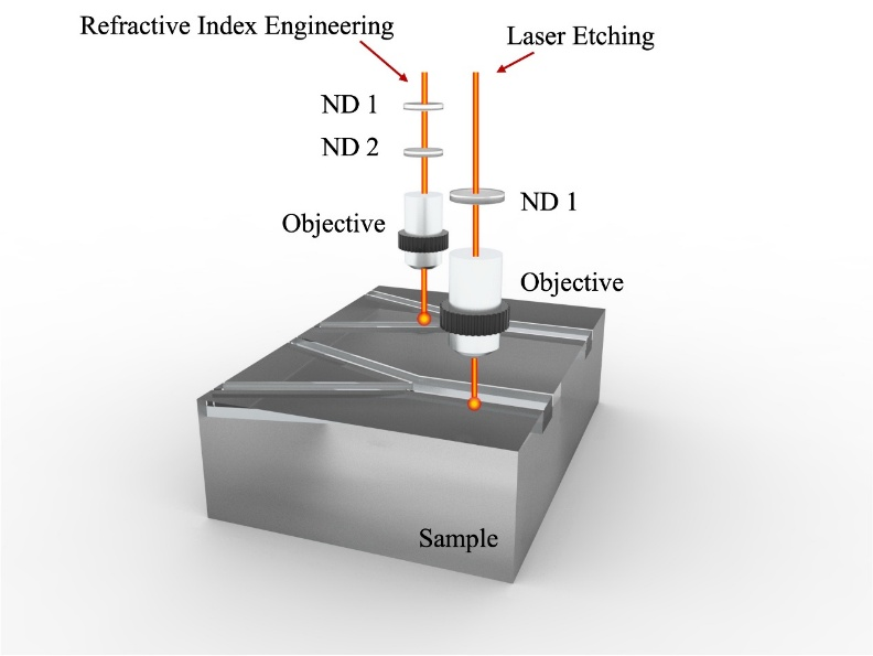
Figure 1 Femtosecond laser etching and refractive index engineering process for samples.
The fabrication of the superficial structures involved a two-step process, utilizing different objectives and laser parameters to achieve the desired structural features as shown in Figure 1. Initially, the laser beam was focused 30 μm beneath the largest surface of the wafer (10 mm × 9.8 mm). A series of tests were conducted at various pulse energies and scanning velocities to optimize the fabrication conditions. Optical microscopy in transmission mode was employed to assess the damage tracks created within the sample. Based on these evaluations, the final irradiation parameters were set to a pulse energy of 100 μJ, achieved through the use of two neutral density filters.
During the irradiation process, the sample was moved at a constant speed of 500 μm/s in a direction perpendicular to both the laser polarization and the pulse propagation. This direction was carefully aligned with the 10-mm long edge of the sample to produce a continuous damage track along its length. The optimal values for scanning velocity and pulse energy were determined through a careful balance between achieving sufficient damage in the laser tracks (to create a high refractive index contrast) and minimizing the formation of cracks within the sample. Multiple parallel scans were performed, with adjacent damaged tracks separated by approximately 3 μm, forming the bottom boundaries of the superficial structures.
In the second step, a multi-scan strategy was employed to create the side-walls of the superficial structures. A single neutral density filter was used to increase the pulse energy to 150 μJ. Under these conditions, the estimated peak fluence reached approximately 700 J/cm2, which is significantly higher than the typical ultrafast etching thresholds for transparent dielectrics (a few J/cm2). This high fluence indicated that the process was operating in the strong etching regime, which allowed us to bypass the saturation effect commonly observed in etching craters.
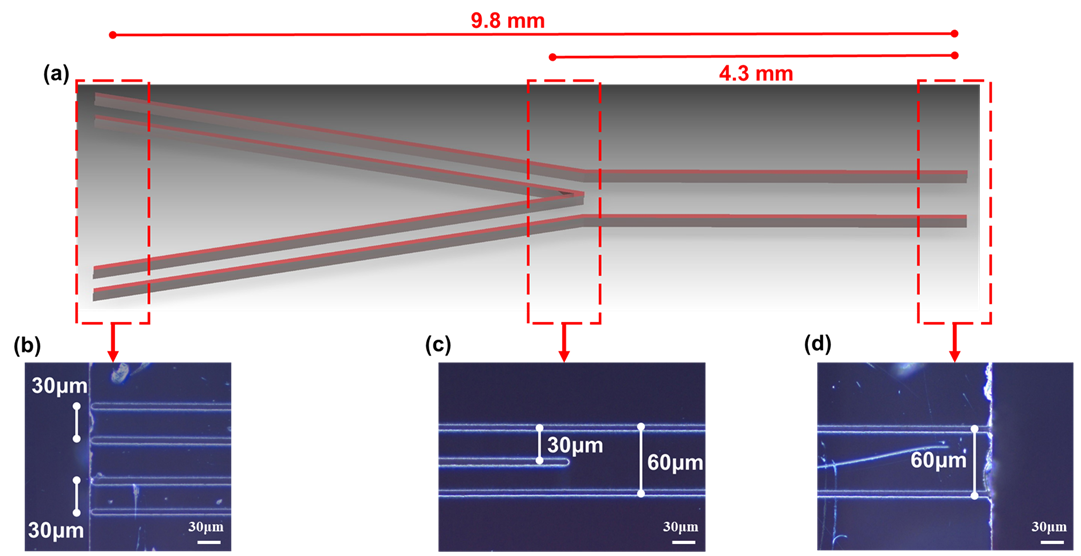
Figure 2 (a) The sketch of Y-branch etching tracks on the top view. (b) The microscope image of Y-branch output port. (c) The microscope image of Y-branch joint. (d) The microscope image of Y-branch and input port.
The Y-branch waveguiding structure was produced following this procedure. The design consists of a straight bus waveguide (i.e. w width) that is split into two divergent identical waveguides (w/2 width). An angle (in this work the value is 0.05 deg) is fixed between the two split waveguides, ensuring a distance of 30 μm between the two output ports of the Y-branch at the end-face. The design is similar to the rectangle cladding waveguides, instead of writing side-walls of etchings. The sketch of the waveguide splitter is shown in Figure 2(a), which shows the details of Y-branch structure. For steadily exciting the guiding mode, a 4.3-mm-long straight bus waveguide and 5.5-mm-long split channels are carefully chosen. Figure 2(b)-Figure 2(d) are demonstrated the microscope images of output port, joint, and input port, respectively, in the top view. The microphotograph of the input and output port cross-sections is demonstrated in Figure 3(a), Figure 3(b).
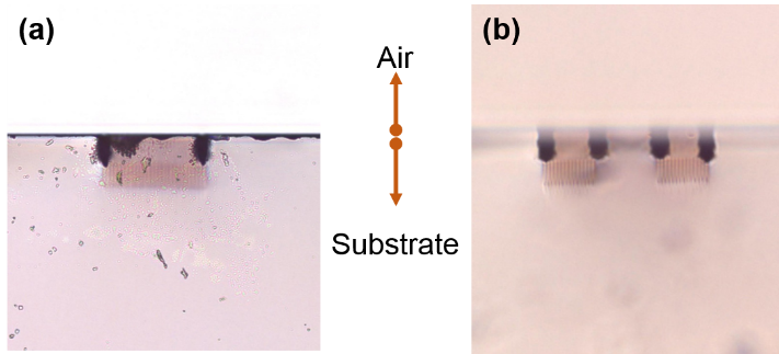
Figure 3 (a) Microphotographs of Y-branch splitter input ports. (b) Microphotographs of Y-branch splitter output ports.
To investigate the near-field modal distributions of Y-branch waveguiding structure, a typical end-face coupling system was employed. A 1550-nm fiber DFB laser source with a polarization controller, using a fiber collimator to set light off from the fiber to the free space, was coupled into one end-face of the LiTaO3 sample by an objective lens. Another microscope objective lens was used as the out-coupler through which the transmitted light was collected and imaged by a camera. The polarization controller and a Glan-Taylor prism were set to ensure the linear polarized light output from the collimator. A half-wave plate was inserted after the Glan-Taylor prism to adjust the direction of the polarization. Applied a power meter, the dependency of input light polarization and output power is measured by a power meter. For obtaining the power from each output port, an aperture was used to limit only one port output light passed by.
3. Results and discussion
Figure 4(a) presents the measured output near-field modal profile of the Y-branch splitter at a telecommunication wavelength of 1.55 μm. The dashed lines in the figure indicate the air-crystal interface and the waveguiding cores. The output light field modal profiles from each exit port exhibit a Gaussian-like distribution. The refractive index change induced by the femtosecond laser writing tracks at the bottom of the waveguiding structure was estimated to be -0.005 in the LiTaO3 (LT) crystal, consistent with the existing experimental value.[25] We hypothesize that the femtosecond laser etching creates void grooves at the crystal surface, resulting in a refractive index of approximately 1.0, similar to that of a vacuum.
To simulate the light propagation through the Y-branch structure, we established a refractive index distribution based on the calculated refractive index modifications. The simulation was performed using the Finite-Difference Beam Propagation Method (FD-BPM) algorithm implemented in Rsoft® BeamPROP software. Figure 4(b) displays the simulated output near-field modal profile. The slight discrepancy between the experimental results and the simulation is attributed to the surface roughness of the superficial structures induced by femtosecond laser etching.
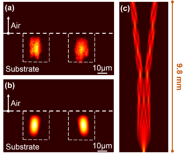
Figure 4 (a) The measured output near-field modal profiles. (b) The simulated output near-field modal profiles. (c) The simulated exciting light field profile of Y-branch waveguiding structure in the top view.
Figure 5 illustrates the output power distribution (in mW) of all-angle transverse-plane light transmission at a wavelength of 1550 nm. In the experiment, 3 mW of circularly polarized light was injected into the hybrid waveguide structure via an end-face coupling system, and the output power was measured at various angles. The results reveal significant angular-dependent variations in output power: distinct peaks (approximately 250-300 μW) are observed at 180°, while lower values (around 50-100 μW) appear near 0°. This anisotropic distribution is closely related to the polarization sensitivity of the waveguide. It exhibits higher transmission efficiency for TE-polarized light. Furthermore, as a critical factor in the performance of waveguides, the propagation losses of waveguides in lithium tantalate (LiTaO₃) crystals were estimated. The total losses of the straight bus waveguides (including both propagation and coupling losses) were measured at a wavelength of 1550 nm using an end-face coupling system. This type of loss can be characterized as Insertion Loss(IL),
Considering the Fresnel reflection, a loss of -0.65 dB occurs at each waveguide–air interface. For the 4.3-mm-long straight bus waveguides, the propagation losses in the transverse electric (TE) polarization direction were as low as approximately 9.6 dB/cm. The disparity in propagation losses (4.8 dB/cm for the tracks) contributes to the asymmetry in power distribution. These results demonstrate that the hybrid waveguide achieves polarization-dependent spatial power allocation through laser-induced refractive index anisotropy (∆n0), offering a viable solution for integrated polarization beam-splitting devices.
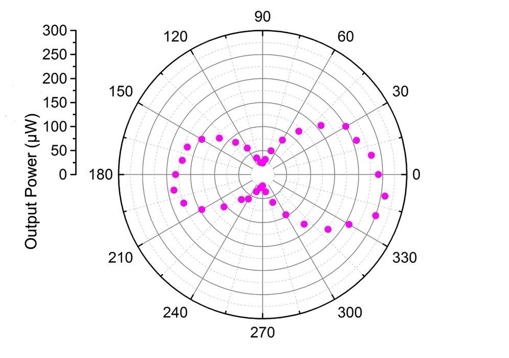
Figure 5 All-angle light transmission along the transverse plane at 1550 nm.
4. Conclusion
In this study, we successfully fabricated a Y-branch superficial superficial waveguide splitter in a LiTaO3 crystal wafer using a combination of femtosecond laser writing and ablating techniques. The hybrid approach leveraged the precision and flexibility of femtosecond laser technology to create high-quality waveguides with well-defined geometries. The fabricated Y-branch waveguide splitter exhibited remarkable polarization sensitivity and superior waveguiding performance, particularly at the telecommunication wavelength of 1.55 μm.
The experimental results demonstrated that the Y-branch waveguide splitter achieved an output power splitting ratio of approximately 1:1, with Gaussian-like modal profiles observed at the output ports. The refractive index change induced by the femtosecond laser writing tracks was estimated to be -0.005, consistent with previous reports. The polarization sensitivity of the waveguide was evidenced by the significant angular-dependent variations in output power, with higher transmission efficiency observed for TE-polarized light.
In this study, we have also conducted a comparative analysis between the hybrid femtosecond laser fabrication technique employed in our work and several conventional waveguide fabrication methods, such as thermal diffusion, proton exchange, and ion implantation. Compared to these traditional approaches, our method demonstrates notable advantages in terms of both processing flexibility and structural accuracy. By integrating femtosecond laser direct writing with precision-controlled ablation, we are able to fabricate waveguide structures with well-defined geometries and smooth sidewalls in a streamlined, mask-free process.[26-27] This not only simplifies the overall fabrication procedure but also enhances the reproducibility and uniformity of the devices. Moreover, the hybrid approach allows for highly localized, design-flexible fabrication, making it particularly well-suited for constructing compact and polarization-sensitive photonic components.[28] We believe that these strengths collectively highlight the superior performance and practical applicability of our fabrication strategy in comparison with conventional techniques.
The combination of femtosecond laser etching and refractive index engineering allowed for the creation of a superficial guiding structure with precise control over the side-walls and bottom boundaries. This unique structure exhibited polarization-dependent spatial power allocation through laser-induced refractive index anisotropy, offering a viable solution for integrated polarization beam-splitting devices. The excellent waveguiding performance at 1.55 μm wavelength ensures efficient transmission and minimal loss, making this Y-branch splitter a promising candidate for integration into advanced photonic devices and systems.
Conflicts of Interest
The authors declare no conflict of interest.
Acknowledgements
This work was supported by the Shandong Province Scientific and Technological Achievement Transfer and Transformation Subsidy (Shandong-Chongqing Science and Technology Cooperation) Project.
Author contributions
Quanhong Feng and Zhenghao Liu: Formal analysis, Investigation, Software, Visualization, Writing-Original Draft;
Dongying Hou: Visualization, Writing-Original Draft;
Chen Cheng: Corresponding author, Project administration, Supervision, Validation.
References
-
D. Zhu, L. Shao, M. Yu, R. Cheng, B. Desiatov, C. Xin, Y. Hu, J. Holzgrafe, S. Ghosh, A. Shams-Ansari, E. Puma, N. Sinclair, C. Reimer, M. Zhang, M. Lončar. "Integrated photonics on thin-film lithium niobate." Advances in Optics and Photonics. 2021, 13, 242-352.
-
C. Hu, A. Pan, T. Li, X. Wang, Y. Liu, S. Tao, C. Zeng, J. Xia. "High-efficient coupler for thin-film lithium niobate waveguide devices." Optics Express. 2021, 29, 4, 5397-406.
-
Y. Xie, P. Wang, H. Yu, C. Zhong, J. Peng, J. Wang, C. Yang, Y. Han, A. Li, Z. Guan, F. Qiu, and M. Li. "PZT photonic materials and devices platform." Journal of Semiconductors. 2024, 45, 12, 120501.
-
G. Chen, N. Li, J. Ng, H. Lin, Y. Zhou, Y. Fu, L. Lee, Y. Liu, A. Danner. "Advances in lithium niobate photonics: development status and perspectives." Advanced Photonics. 2022, 4, 3, 034003.
-
C. Wang, M. Zhang, B. Stern, M. Lipson, M. Lončar. "Nanophotonic lithium niobate electro-optic modulators." Optics Express. 2018, 26, 2, 1547-1555.
-
M. Bazzan, C. Sada. "Optical waveguides in lithium niobate: Recent developments and applications." Applied Physics Reviews. 2015, 2, 4, 040603.
-
J. Fassbender, J. McCord. "Magnetic patterning by means of ion irradiation and implantation." Journal of Magnetism and Magnetic Materials. 2008, 320, 3–4, 579-596.
-
Q. Luo, F. Bo, Y. Kong, G. Zhang, J. Xu. "Advances in lithium niobate thin-film lasers and amplifiers: a review." Advanced Photonics. 2023, 5, 3, 034002.
-
Q. Zhu, Y. Wang, X. Shen, H. Guo, C. Liu. "Optical Ridge Waveguides in Magneto-Optical Glasses Fabricated by Combination of Silicon Ion Implantation and Femtosecond Laser Ablation." IEEE Photonics Journal. 2018, 10, 5, 2400507.
-
K. Davis, K. Miura, N. Sugimoto, K. Hirao. "Writing waveguides in glass with a femtosecond laser." Optics Letters. 1996, 21, 21, 1729–1731.
-
R. Gattass, E. Mazur. "Femtosecond laser micromachining in transparent materials." Nature Photonics. 2008, 2, 219–225.
-
Y. Jia, S. Wang, F. Chen. "Femtosecond laser direct writing of flexibly configured waveguide geometries in optical crystals: fabrication and application." Opto-Electronic Advances. 2020, 3, 10, 190042.
-
A. Okhrimchuk, A. Shestakov, I. Khrushchev, J. Mitchell. "Depressed cladding, buried waveguide laser formed in a YAG:Nd³⁺ crystal by femtosecond laser writing." Optics Letters. 2005, 30, 17, 2248–2250.
-
J. Burghoff, C. Grebing, S. Nolte, A. Tünnermann. "Efficient frequency doubling in femtosecond laser-written waveguides in lithium niobate." Applied Physics Letters. 2006, 89, 081108.
-
P. Nge, I. Chad, Rogers, T. Adam, Woolley. "Advances in microfluidic materials, functions, integration, and applications." Chemical Reviews. 2013, 113, 4, 2550-2583.
-
X. Wang, R. Liu, Y. He, Y. Fu, J. Wang, A. Li, X. Guo, M. Wang, W. Guo, T. Zhang, Q. Shu, Y. Yao. "Determination of detonation characteristics by laser-induced plasma spectra and micro-explosion dynamics." Optics Express. 2022, 30, 4, 4718-4736.
-
S. Juodkazis, K. Nishimura, S. Tanaka, H. Misawa, E. Gamaly, B. Luther-Davies, L. Hallo, P. Nicolai, V. Tikhonchuk. "Laser-induced microexplosion confined in the bulk of a sapphire crystal: Evidence of multimegabar pressures." Physical Review Letters. 2006, 96, 16, 166101.
-
J. Wang, Y. Song, B. Dong, Y. Zhao, Q. Sun, M. Yan, C. Yao, Q. Du, Z. Xu. "Femtosecond laser controllable annealing for color centers based on ion-implanted silicon carbide substrate." Ceramics International. 2024, 50, 22, 46566-46578.
-
R. S. Weis, T. K. Gaylord. "Lithium niobate: Summary of physical properties and crystal structure." Applied Physics. 1985, 37, 4, 191-203.
-
A. Boes, B. Corcoran, L. Chang, J. Bowers, A. Mitchell. "Status and potential of lithium niobate on insulator (LNOI) for photonic integrated circuits." Laser & Photonics Reviews. 2018, 12, 4, 1700256.
-
A. Butkutė, L. Jonušauskas. "3D manufacturing of glass microstructures using femtosecond laser." Micromachines. 2021, 12, 5, 499.
-
T. Lee, Q. Sun, M. Beresna, G. Brambilla. "Low bend loss femtosecond laser written waveguides exploiting integrated microcrack." Scientific Reports. 2021, 11, 1, 23770.
-
M. Vazimali, S. Fathpour. "Applications of thin-film lithium niobate in nonlinear integrated photonics." Advanced Photonics. 2022, 4, 3, 034001.
-
J. Wang, Y. Song, B. Dong, Y. Zhao, Q. Sun, M. Yan, C. Yao, Q. Du, Z. Xu. "Femtosecond laser controllable annealing for color centers based on ion-implanted silicon carbide substrate." Ceramics International. 2024, 50, 22, 46566-46578.
-
C. Cheng, Y. Jia, J. Aldana, Y. Tan, F. Chen. "Hybrid waveguiding structure in LiTaO3 crystal fabricated by direct femtosecond laser writing." Optical Materials. 2016, 51, 190-193.
-
Y. Zhu, Q. Wan. "Lithium niobate/lithium tantalate single-crystal thin films for post-moore era chip applications." Moore More. 2024, 1, 1, 6.
-
G. Chen, N. Li, J. D. Ng, H.-L. Lin, Y. Zhou, Y. H. Fu, L. Y. T. Lee, Y. Yu, A.-Q. Liu, A. J. Danner. "Advances in lithium niobate photonics: development status and perspectives." Adv. Photonics. 2022, 4, 3, 034003.
-
B. Zhang, W. Yan, F. Chen. "Recent advances in femtosecond laser direct writing of three-dimensional periodic photonic structures in transparent materials." Adv. Photonics. 2025, 7, 03.