Wet Etching of GaN-Based Optoelectronics: From Fundamental Mechanisms to Advanced Device Integration
published: 18 May 2025 | https://doi.org/10.63174/xdi.LBNT1244
Abstract
GaN-based optoelectronics face persistent challenges, particularly the low light extraction efficiency, which primarily arises from the high refractive index of GaN. This property results in significant internal light reflection at the GaN/air interface, thereby limiting device performance. To mitigate this issue, porous GaN has emerged as a promising solution due to its ability to modify optical properties at the micro- and nanoscale. This paper presents a comprehensive review of wet etching techniques employed for fabricating porous GaN structures, including electrochemical etching, photoelectrochemical etching, and defect-selective etching methods. These approaches are vital for achieving tunable porosity, structural uniformity, and precise control over morphology, which are critical for optimizing device integration and functionality. Furthermore, the mechanisms by which porous GaN enhances light extraction are systematically analyzed. These include refractive index modulation, enhanced light scattering, increased critical angle for total internal reflection, and improved reflectivity through the incorporation of distributed Bragg reflector (DBR) effects. These mechanisms collectively contribute to better out-coupling of generated photons.In addition, the wide-ranging applications of porous GaN are explored, covering ultraviolet light-emitting diodes (UV LEDs), full-color micro-LED displays, high-sensitivity ultraviolet photodetectors, and advanced optical devices such as photonic crystals and optical resonators. Despite its benefits, challenges remain, including the need to fully understand how porous architecture parameters affect device reliability and long-term performance. Future research should emphasize integrated material-structure design strategies and broaden the scope of application in next-generation optoelectronic technologies.
1. Introduction
GaN is a typical wide band gap semiconductor material with a band gap of about 3.4 eV[1], high thermal conductivity, high chemical stability and excellent electron mobility[2][3], and has wide application prospects in the field of high power, high frequency and short wavelength optoelectronic devices[4,5]. GaN crystals are usually wurtzite crystals with extremely strong bonding energy and high chemical inertness[6]. The crystal surface includes Ga polar (0001) plane and N polar (000 - 1) plane, which differ significantly in surface energy, chemical reactivity and defect density[7,8].Among them, the N polar surface is easier to be selectively etched in alkaline solutions such as KOH and NaOH, while the Ga polar surface is almost impossible to be etched under normal conditions[9,10].Due to its chemical stability, GaN is difficult to achieve high-quality structural processing by traditional wet etching[11,12]. To this end, researchers have proposed technical paths such as photoelectrochemical etching (PEC) and electrochemical etching (ECE)[13,14]. PEC generates holes by UV excitation, inducing Ga-N bond breakage and formation of soluble oxidation products (e.g. Ga ˇ O)[15-17], while ECE induces oxidation reactions in the n-type layer by applying an anode bias, thus forming porous structures throughout the doped layer[18,19]. These methods achieve precise regulation of porous GaN while maintaining low damage[20,21].During the formation of porous structure, crystal defects (such as dislocation, vacancy, impurity rich region, etc.) play a significant role in guiding the etching process. The defect energy level is usually located in the middle of the forbidden band, which makes it easier to capture holes and preferentially generate oxidation reactions, thus forming a "defect preferential etching" path[22,23]. This not only changes the spatial selectivity of etching, but also makes the hole distribution highly correlated with dislocation density[24]. In addition, defect-induced stress concentrations also lower the local etch barrier, allowing porous structures to preferentially expand in regions of high defect density[25,26]. By combining PEC with doping control, researchers have achieved multi-scale control of pore size distribution, pore density and pore morphology[27,28].
The effective refractive index of GaN decreases significantly with the introduction of porous structure, which alleviates the abrupt refractive index change at the interface with air (n≈2.4 vs n=1.0)[29,30]. The existence of the holes also improves the scattering efficiency of waveguide mode light and enhances the light extraction ability[31,32]. Furthermore, periodic stacking of porous GaN and dense GaN layers can be used to construct a high reflectivity distributed Bragg reflector (DBR) for wavelength selective feedback[33,34].In terms of stress regulation, porous structure has significant slow release effect. The presence of voids can significantly reduce the effective Young's modulus of the material and reduce residual stresses in heteroepitaxy by dispersing thermal stress paths[35,36]. It has been shown that under the same epitaxial conditions, the stress level of porous GaN structure is much lower than that of traditional dense GaN or AlGaN film layer[37,38], and it can also passivate dislocations and improve epitaxial quality to some extent [39].With the development of porous structure control technology, GaN has shown new application potential in many fields such as photonic crystals, optical resonators, and microsensors. Through the collaborative optimization of defect control and wet etching technology, it is expected to realize high-performance GaN device structures with more functional integration and reliability[40,41].
2. Formation Mechanisms of Porous GaN and Wet Etching Techniques
GaN a typical wide-bandgap semiconductor, consists of a crystal lattice composed of gallium and nitrogen atoms. GaN generally adopts a wurtzite-type hexagonal crystal structure, although the zinc-blende cubic phase can also exist under specific conditions. As illustrated in Figure 1, the unit cell of wurtzite GaN features a hexagonal close-packed atomic arrangement. Each gallium atom is tetrahedrally coordinated by four nitrogen atoms, and each nitrogen atom is similarly surrounded by four gallium atoms. This strong covalent bonding imparts exceptional chemical stability to the GaN crystal, rendering it highly resistant to chemical attack by most acids and bases at room temperature[42].In particular, the Ga-polar surface (c-plane oriented upward) exhibits high surface bond energy and low defect density, making it nearly inert to conventional wet chemical etching under ambient conditions. Effective etching of this surface typically requires photoinduced generation of holes under ultraviolet illumination—known as photoelectrochemical (PEC) etching—or the application of an external anodic bias to drive electrochemical oxidation reactions[43,44]. In contrast, the N-polar surface of GaN is more defect-sensitive and susceptible to anisotropic wet etching under elevated temperatures (e.g., above 90 °C) when exposed to concentrated alkaline solutions such as KOH or NaOH. This etching process can form hexagonal etch pits along specific crystallographic planes; however, it usually requires stringent conditions, including elevated temperature, prolonged immersion, and precise control of alkali concentration [45,46].
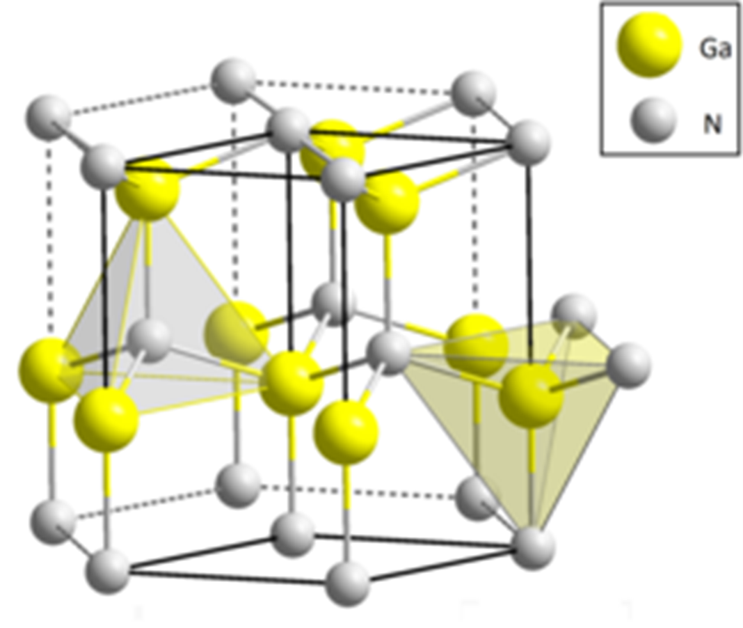
Figure 1. The crystal structure of GaN[45].
In summary, due to the intrinsic chemical stability and inertness of GaN, the formation of porous structures relies on wet etching techniques capable of overcoming these limitations[47,48] .Such methods provide a critical technological foundation for the integration and performance optimization of porous GaN in optoelectronic devices[49,50].
2.1. Electrochemical Etching (ECE)
ECE is a wet etching technique that enables nanoscale structural modulation by inducing selective redox reactions in semiconductor materials under an applied voltage in an electrolyte solution. This method is particularly suitable for n-type GaN due to its high etching rate, minimal damage, large aspect ratio, and environmentally benign processing, and it has become widely adopted for the fabrication of porous GaN structures[51,52].
In 2013, Lee et al. successfully fabricated nanoporous GaN via EC and reported a low band-edge photocurrent barrier of 304 meV, offering design insights for solar cell applications[53]. Cheah et al. systematically investigated the influence of etching time on pore morphology in KOH solutions and found that prolonged etching led to reduced crystal quality[54]. Radzali et al. observed that longer etching durations enhanced pore density, reduced dislocation densities, and improved Raman signal intensity. Kumazaki et al. further refined pore morphology by combining EC with chemical etching[55].Significant progress has also been achieved in China. Shandong University demonstrated the formation of vertically aligned nanopores in n-type GaN using HF or HF/ethanol mixtures, achieving etching rates exceeding 100 μm·min⁻¹[43]. The Chinese Academy of Sciences employed [BMIM]ClO₄ ionic liquids coupled with light-assisted etching to optimize pore morphology and lattice integrity[56,57].During EC, GaN serves as the anode immersed in the electrolyte. Under an externally applied forward bias, holes are injected and induce the breaking of Ga–N bonds, leading to the formation of soluble Ga³⁺ complexes that are subsequently removed from the crystal lattice[58]. This process is highly dependent on the carrier concentration of the material, exhibiting excellent doping selectivity[59]. Common electrolytes include oxalic acid, hydrofluoric acid, and nitric acid. Notably, EC in oxalic acid involves a six-electron transfer mechanism, allowing for the formation of vertically oriented deep pores[60]. The resulting etch morphology is strongly influenced by parameters such as applied voltage, current density, and electrolyte composition—low voltages tend to yield dendritic pores, while higher voltages promote the formation of columnar, through-pore structures[61].Figure 2 illustrates a typical experimental procedure for electrochemical etching of porous GaN: a Si-doped n-type GaN sample with a [100] crystal orientation (1 cm × 0.5 cm) is used as the anode and etched in an oxalic acid solution.
Figure 2. A schematic representation of n-GaN etching in oxalic acid[61].
2.2. Photoelectrochemical Etching (PEC)
PEC is a technique that enables controlled material removal by initiating chemical reactions through light energy, and it has shown particular advantages in the micro- and nanofabrication of wide-bandgap semiconductors such as GaN. For intrinsic or lightly doped GaN, the low intrinsic conductivity limits hole injection, necessitating the use of light to enhance carrier generation—a process referred to as photoelectrochemical etching[39]. In PEC, the sample is illuminated with ultraviolet or near-ultraviolet light to excite valence band electrons and generate holes. These photo-generated holes, driven by the anodic electric field, migrate to the surface and oxidize the GaN upon reacting with the electrolyte. Compared with purely electrochemical etching, PEC offers better control over the etching of lightly doped or intrinsic layers and is commonly used to form nanoporous arrays on Ga-polar surfaces or within heterostructures. The PEC process is highly sensitive to several parameters, including the pH of the electrolyte, light intensity, and wavelength. In 2019, Lu X. et al. proposed an innovative two-step etching approach that incorporated a SiO₂ sidewall protection layer (SPL), effectively safeguarding the n-type semiconductor layers and the LED active region from electrolyte-induced damage. Compared to untreated standard LED samples, the SPL-based DBR-LED exhibited a 54.3% increase in peak external quantum efficiency (EQE) and a 65.7% enhancement in optical output power at 100 mA, with no observable degradation in electrical performance. The photoelectrochemical etching device is shown in Figure 3 below.
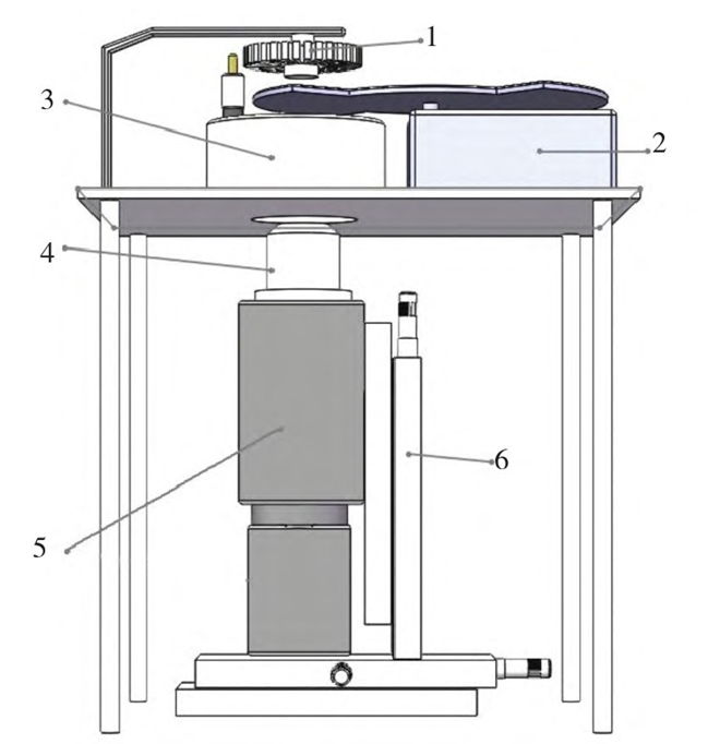
Figure 3. Schematic Diagram of Photoelectrochemical Micro-nano Fabrication Device[56].
Figure 4 shows the surface and cross-sectional SEM images of porous GaN layers with varying porosity obtained after photoelectrochemical etching. Furthermore, the study by Lu, X. et al. demonstrated that the etching process is strongly influenced by the doping concentration in n-type GaN[39].
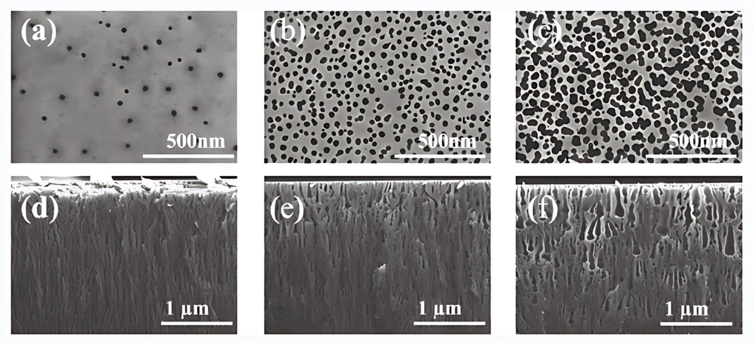
Figure 4. Surface and cross-sectional SEM images of porous GaN layers with different porosities.
The SEM images reveal the porous network consisting of void regions (dark areas) and a nanocrystalline GaN framework (bright areas), which optically form a low-refractive-index layer that effectively scatters incident light and enhances light extraction efficiency.
2.3. Defect-Selective Etching (DSE)
DSE is a technique that leverages the enhanced chemical reactivity at defect sites—such as dislocations and vacancies—within GaN crystals to enable localized etching. These defect-rich regions exhibit higher chemical activity and are therefore more susceptible to corrosion under specific chemical environments, even in the absence of an applied voltage. For example, when GaN samples are immersed in heated KOH or NaOH solutions, hexagonal etch pits preferentially form at screw and edge dislocations, thereby “revealing” the dislocation distribution on the surface[62]. Although DSE does not generate a continuous porous network, it is well-suited for roughening the emission surface of LEDs to enhance light scattering. Scanning electron microscopy (SEM) can be used to directly visualize the etching morphologies on GaN surfaces with different polarities (metal-polar vs. N-polar)
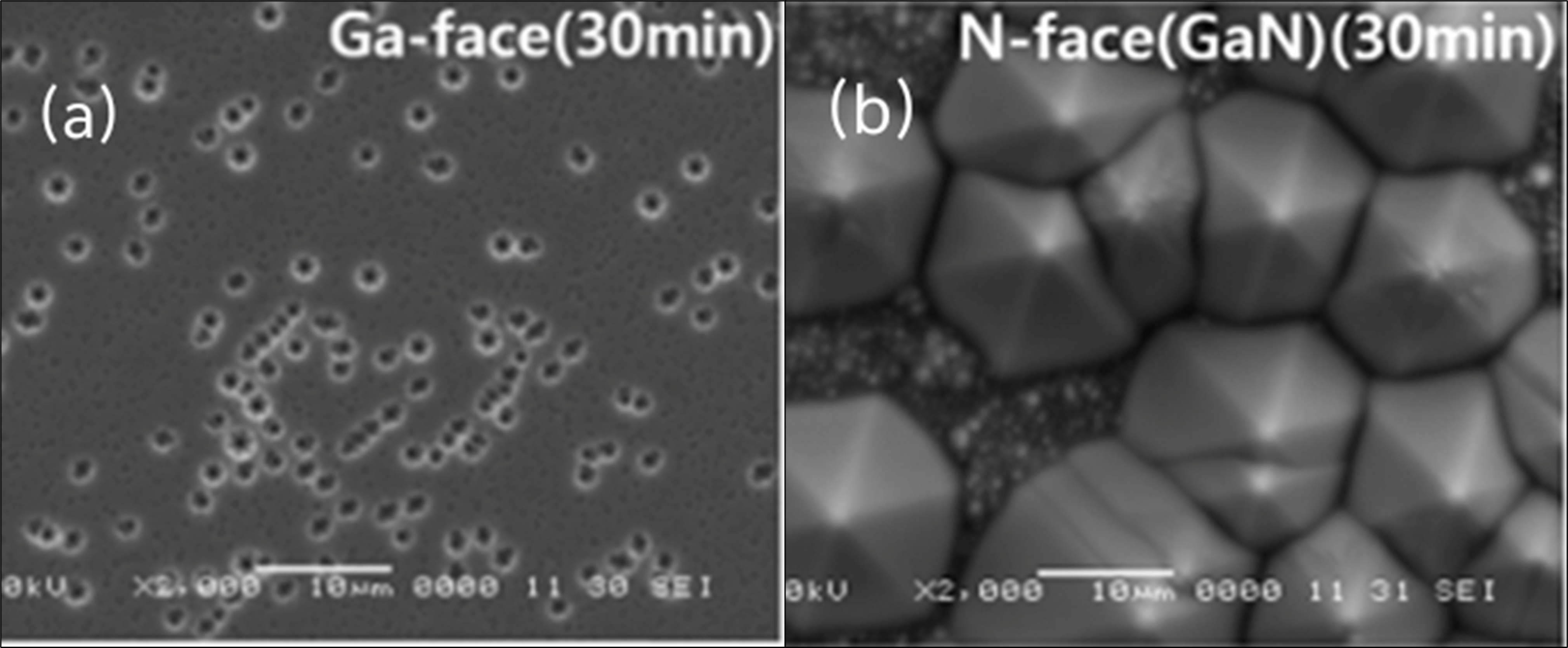
Figure 5. (a) Etching morphology of Ga-polar surface; (b) Etching morphology of N-polar surface of GaN[62].
3. Mechanisms of Light Extraction Enhancement by Porous Structures
To fully understand the functional advantages of porous GaN in optoelectronic devices, it is essential not only to investigate its fabrication methods, but also to explore how its structural features contribute to enhanced optical performance. Building upon the understanding of the formation mechanisms and etching techniques introduced earlier, the following chapter focuses on the physical principles through which porous structures enhance light extraction efficiency. These mechanisms also lay the theoretical foundation for the practical device applications discussed in subsequent sections.
3.1. Refractive Index Modulation and Anti-Reflection Function
GaN exhibits a high refractive index (n ≈ 2.4) in the ultraviolet spectral range, resulting in a strong refractive index mismatch with air (n = 1.0). This leads to significant Fresnel reflection and total internal reflection at the emission interface. In a study by Chandramohan et al. (2021), the authors embedded air-void structures within GaN to effectively modulate its effective refractive index and internal stress, thereby substantially enhancing the light extraction efficiency and overall performance of UV LEDs.Porous GaN, as an "effective medium," exhibits an intermediate refractive index between that of GaN and air[63]. Its effective index can be tuned via porosity control, enabling the formation of a gradient refractive index (GRI) profile[64]. For instance, a porous GaN layer with 40% porosity may have a refractive index reduced to approximately 1.8, effectively lowering the reflection at the GaN/air interface from 34% to around 10%[65]. The implementation of multilayered GRI structures—such as continuously graded porosity or pore-size gradient designs—can further suppress interference fringes and reflection losses, functioning similarly to anti-reflection coatings[66]. Figure 6 clearly illustrates the effect of different fill factors on photoluminescence (PL) intensity.
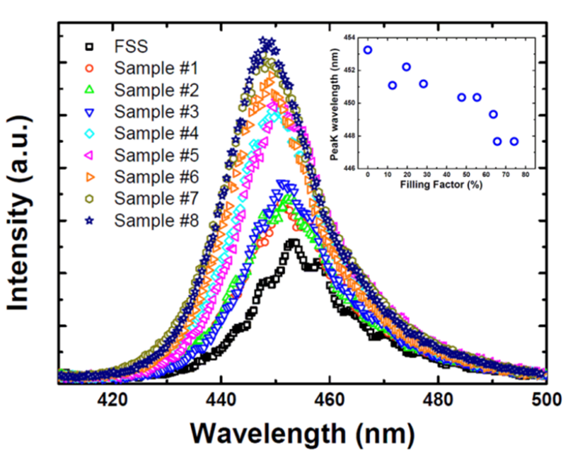
Figure 6. Comparison of photoluminescence (PL) intensity between FSS-LED and LDPSS-LED samples[66].
Figure 6 compares the photoluminescence (PL) intensity of conventional flat sapphire substrate LEDs (FSS-LED) with those of laser-patterned sapphire substrate LEDs (LDPSS-LED) under different filling factors (FF). The experimental results show that the LDPSS-LED samples exhibit significantly enhanced emission intensity across the entire wavelength range (420–500 nm) compared to the FSS-LED. Moreover, the PL intensity increases progressively with FF, reaching a maximum enhancement of approximately 140% for Sample #8 relative to the FSS-LED. This indicates that the periodic concave structures effectively enhance light scattering and coupling, thereby improving light extraction efficiency.The inset in the figure 6 further reveals a slight redshift in the PL peak wavelength—from approximately 451 nm to 454 nm—as the FF increases. This redshift may be attributed to stress relaxation in the quantum wells or subtle band structure modifications induced by the patterned substrate. These findings suggest that the LDPSS structure not only boosts light extraction efficiency but may also influence the underlying emission mechanisms.
In addition, the embedded air voids act as stress-relief channels, effectively mitigating the lattice mismatch between GaN and the substrate. This reduces dislocation density and improves the crystalline quality of the epitaxial layer. Such a structure not only enhances the emission efficiency of the device but also improves its long-term stability and reliability, demonstrating significant potential for application in high-efficiency UV LED designs. Figure 7 presents a comparison of the E₂(high) Raman mode spectra between LDPSS-LED and FSS-LED samples, which can be used to evaluate the residual stress state in the crystal structure. The E₂(high) peak of the FSS-LED sample is located at 570.2 cm⁻¹, while that of the LDPSS-LED is slightly red-shifted to 569.8 cm⁻¹. Since the E₂(high) mode is highly sensitive to lattice stress, the observed redshift indicates a notable reduction in compressive stress within the GaN epilayer induced by the LDPSS structure. This stress relaxation contributes to improved crystalline quality and reduced dislocation density, thereby enhancing the emission efficiency and reliability of the LED device. These findings further validate the structural advantages of laser-patterned substrates in improving LED performance.
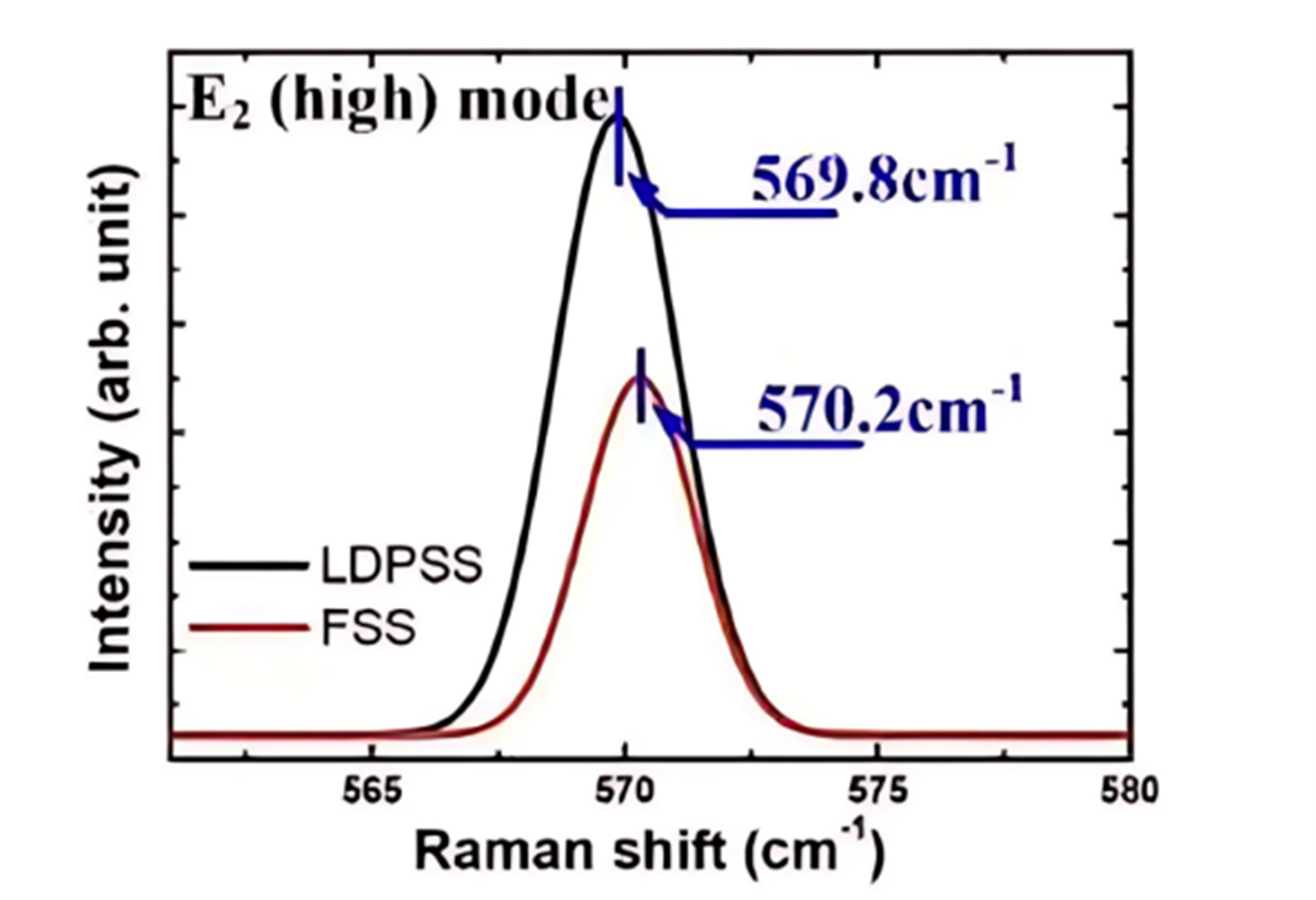
Figure 7. Raman spectral comparison of LDPSS-LED and FSS-LED under the E₂(high) vibrational mode[67].
3.2. Scattering Enhancement and Waveguide Mode Decoupling
In LEDs, a significant portion of the emitted light exists in the form of guided modes confined between the quantum well layers and the electrodes, with most photons trapped inside the chip structure[67]. Porous structures introduce abundant nanoscale irregularities and pore boundaries that induce Rayleigh and Mie scattering of incident light. These scattering mechanisms randomize the propagation direction of waveguided light, allowing more photons to deviate from the original guided path. Once these scattered photons exceed the critical angle, they can escape through the device surface, thereby enhancing light extraction[68].Figure 8 illustrates various propagation paths of light emitted from the n-GaN region, showing how the presence of porous GaN leads to scattering and directional redistribution of the emitted photons.
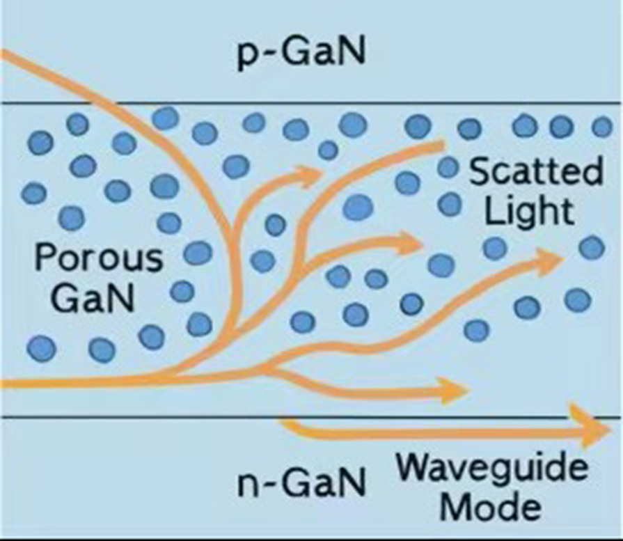
Figure 8. Mechanism of porous GaN in scattering and waveguide mode decoupling.
Additional studies have shown that LEDs incorporating porous surface structures exhibit far-field angular emission profiles that more closely resemble the ideal Lambertian distribution, thereby enhancing the intensity of light emitted in the forward direction[69]. Moreover, the scattering mechanism facilitates the coupling and conversion of Transverse Magnetic (TM) modes into transverse electric (TE) modes, which is particularly beneficial for alleviating the TM-mode dominance commonly observed in deep-ultraviolet (DUV) LED[70].The Transverse Magnetic (TM) mode, on the other hand, is a type of optical mode in which the magnetic field is entirely transverse to the direction of propagation, while the electric field has a longitudinal component. In deep-ultraviolet (DUV) LEDs, TM modes dominate due to the anisotropic crystal orientation of AlGaN materials. However, TM-polarized light tends to propagate laterally, leading to poor vertical emission. Introducing porous GaN structures can enhance scattering, enabling partial conversion of TM modes into Transverse Electric (TE) modes and improving the vertical extraction of light. The mechanisms by which porous GaN structures contribute to improved light extraction efficiency in LEDs are summarized as follows:
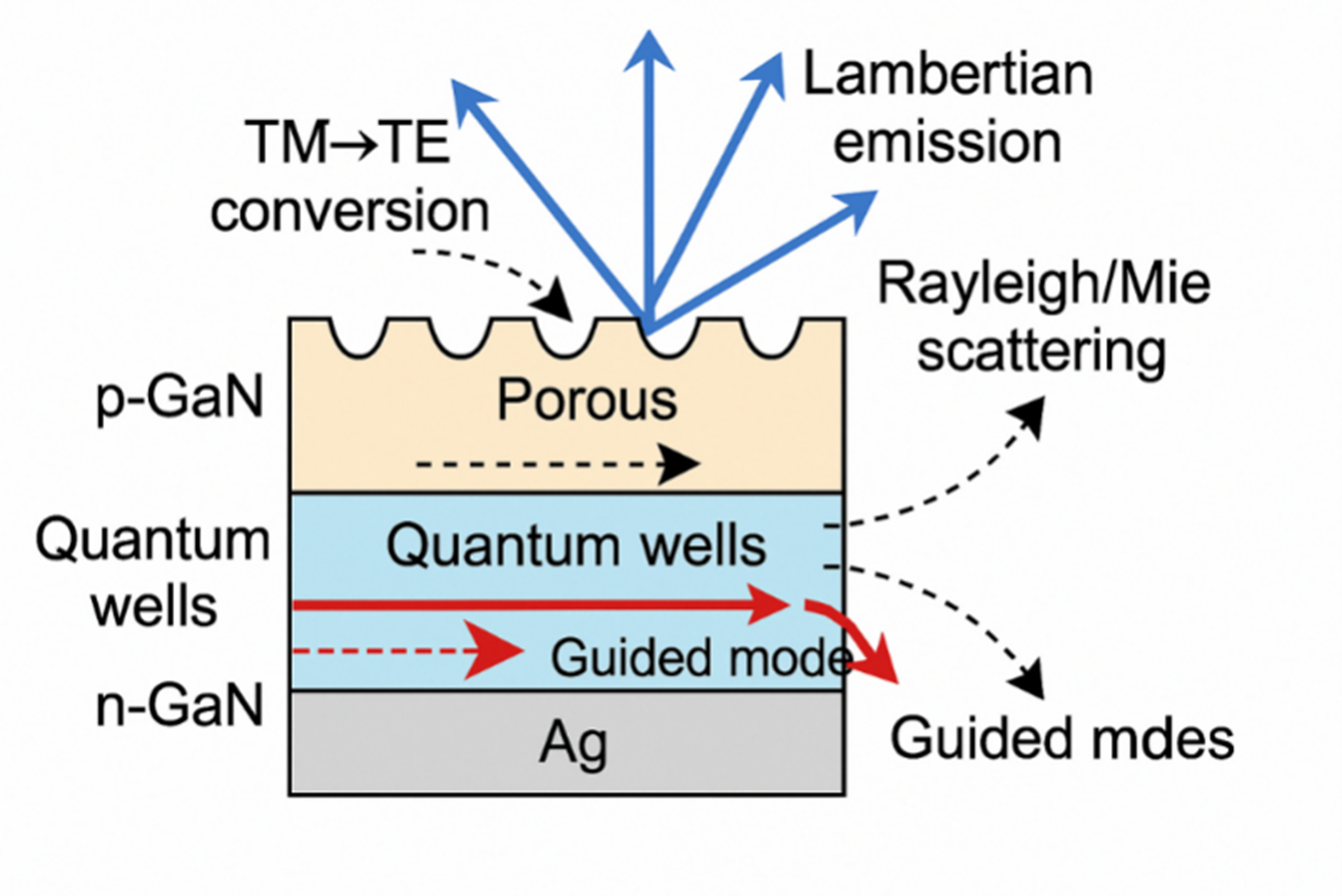
Figure 9. Mechanisms by which porous GaN structures enhance light extraction efficiency in LEDs.
3.3. Increasing the Critical Angle and Reducing Total Internal Reflection
In light-emitting devices, light propagating from a high-refractive-index material (such as GaN) to a lower-index external medium (such as air or encapsulant) undergoes total internal reflection when the incident angle exceeds the critical angle, defined as θ_c = arcsin(n₂/n₁). At the GaN–air interface, the critical angle is only about 24°. By introducing a porous GaN layer as an intermediate medium, the refractive index n₁ can be effectively reduced from 2.4 to approximately 1.7–1.9, thereby increasing the critical angle to above 35–45°[35]. This allows a greater range of internal light angles to escape through the interface rather than being reflected back into the chip, thus enhancing light extraction efficiency. Additionally, employing a multilayer structure with controlled porosity to form a Gradient Refractive Index (GRIN) interface can further expand the extraction cone angle. The conceptual schematic is shown in Figure 10.The Gradient GRIN structure refers to an optical medium in which the refractive index changes gradually across space, rather than remaining uniform. In the context of porous GaN, this is achieved by controlling the porosity distribution to create a smooth refractive index transition between GaN and air. Such a structure significantly reduces Fresnel reflection at the interface and enhances light extraction by minimizing abrupt optical discontinuities.
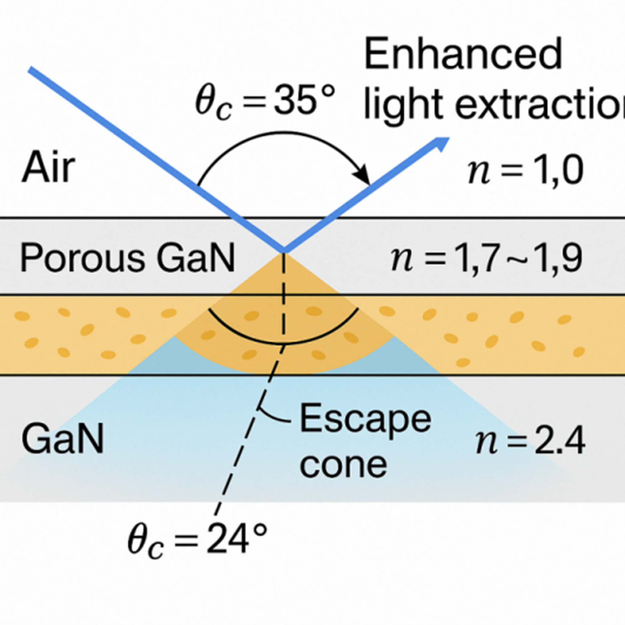
Figure 10. Multilayer porosity-controlled structure for increasing the critical angle and reducing total internal reflection.
3.4. Distributed Bragg Reflection (DBR) Enhancement
Alternating layers of porous GaN and AlGaN can be stacked to form a periodic refractive index profile, enabling the construction of DBRs. When the thickness of each layer satisfies the optical quarter-wavelength condition (λ/4n), strong constructive interference occurs, reflecting downward-propagating light back into the emission region and thus achieving unidirectional light output[71]. Traditional GaN/AlN or AlGaN/GaN DBRs suffer from limited refractive index contrast (Δn < 0.4), typically requiring more than 20 layer pairs to attain high reflectivity. In contrast, the Δn between porous and dense structures can exceed 1.0, allowing reflectivities greater than 95% to be achieved with only 5–8 pairs. This significantly reduces process complexity and thermal stress within the device[35].For instance, in 2019, Lu X. et al. fabricated a DBR by alternately growing n⁺-AlGaN and intrinsic AlGaN layers, followed by anodic etching of the n⁺ layers in HNO₃ under a 15 V bias. The resulting DBR exhibited a reflectivity of 93.5% at 365 nm, and the LED's external quantum efficiency (EQE) was enhanced by over 50%. The reflectance spectrum of the porous AlGaN DBR is shown in Figure 11.
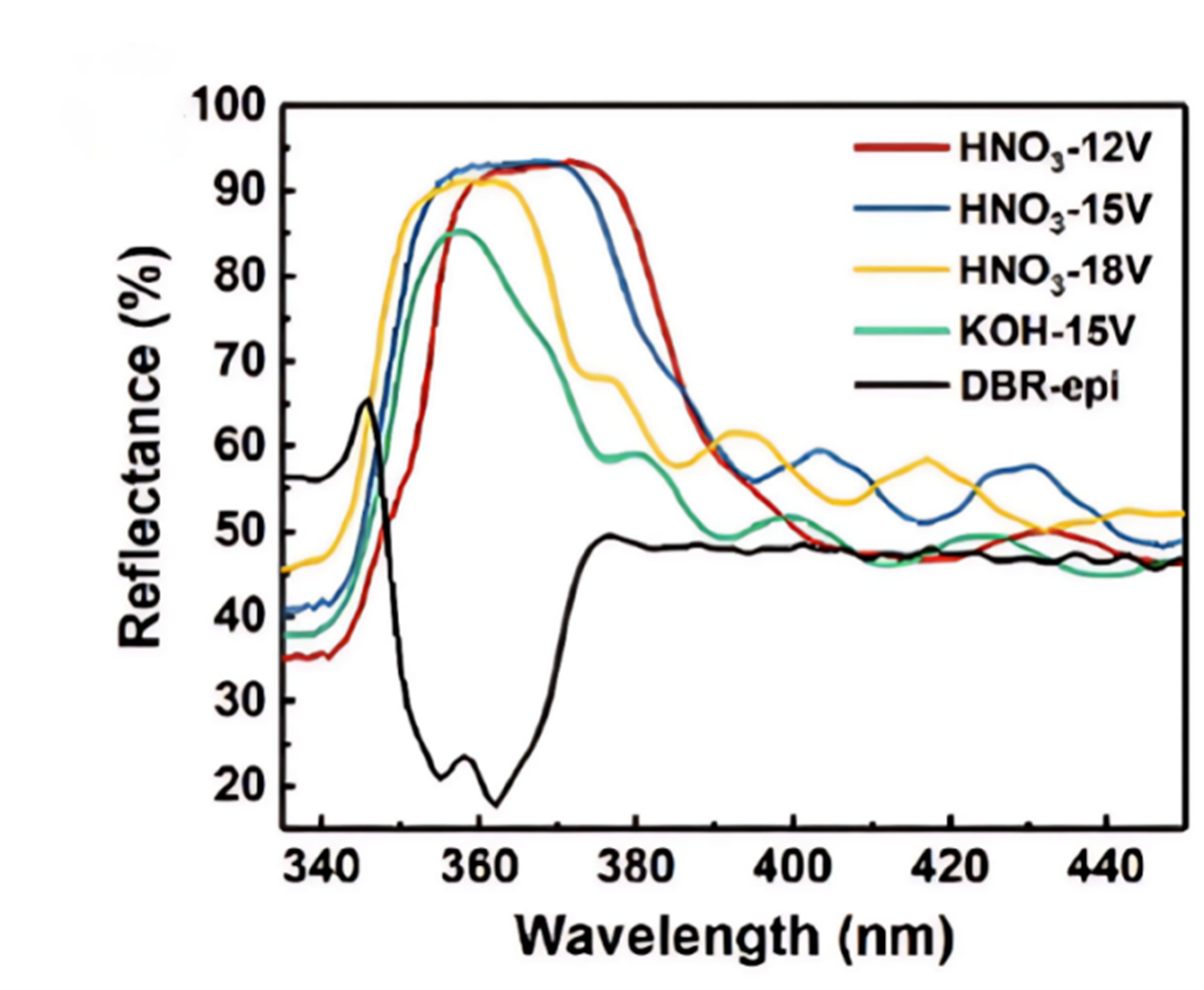
Figure 11. Reflectance spectra of porous AlGaN DBRs etched in HNO₃ and KOH solutions[39].
Figure 11 demonstrates that under a 15 V bias, a porous AlGaN DBR fabricated via electrochemical etching in HNO₃ achieved a peak reflectivity of 93.5% at a wavelength of 365 nm, with a bandwidth of 20 nm[72,73] . This sets a record for the highest reflectivity of porous AlGaN DBRs in the sub-370 nm spectral range. Notably, only 15.5 pairs of u-Al/n⁺-Al layers were required, compared to approximately 40 pairs needed for conventional AlGaN/GaN DBRs.As the applied voltage increased from 12 V to 18 V, the refractive index of the porous layers decreased, leading to a blue shift in the reflectance spectrum[74]. However, at 18 V, the DBR approached the band-edge absorption of Al₉% GaN, resulting in a narrower reflectance bandwidth and a decrease in peak reflectivity[75].
4. Advances in the Application of Porous GaN for Light Extraction Enhancement and Integrated Devices
While the preceding chapter systematically elucidates the fundamental mechanisms through which porous GaN enhances light extraction—such as refractive index modulation, scattering, and DBR-based reflection—the translation of these principles into real-world optoelectronic applications requires careful structural design and integration strategies. In the following section, we examine how these optical advantages are leveraged across diverse device architectures, showcasing the practical implementations and performance gains enabled by porous GaN in ultraviolet LEDs, micro-LED displays, UV photodetectors, and photonic crystal structures[76,77].
4.1 Application of Porous GaN for Enhancing Light Extraction Efficiency in Ultraviolet LEDs
In recent years, porous GaN technology has been extended to various emerging integration directions in ultraviolet LED devices, ranging from charge transport management to optical cavity engineering[78].Firstly, in terms of charge management, the introduction of porous structures can optimize current spreading and carrier injection[79]. By incorporating porous regions within the n-GaN or p-GaN layers, structures resembling current-spreading layers or tunnel junctions can be formed, thereby reducing current crowding and improving hole injection efficiency[80,81].For example, in one study, a highly doped porous GaN tunnel junction was introduced into an AlGaN ultraviolet LED as a transparent electrode to achieve uniform large-area injection. Electroluminescence (EL) spectra of the porous DBR-based UV LED and the conventional structure were compared under different injection current conditions (Figure 12), demonstrating significant improvements in current spreading and output power[79].Furthermore, the incorporation of porous layers can reduce the resistance of the p-type layer, facilitating carrier injection into the active region and thereby suppressing electron overflow and enhancing radiative recombination efficiency [81].
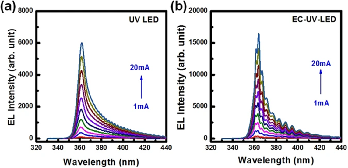
Figure 12. Electroluminescence (EL) spectra of (a) conventional UV-LED and (b) EC-UV-LED fabricated with electrochemically etched porous GaN structures[7].
Secondly, porous GaN contributes significantly to interface passivation and carrier management. Owing to its large internal surface area, the porous structure facilitates the formation of a thin native oxide layer on the pore walls, enabling effective surface passivation[82]. In ultraviolet photodetectors, self-passivation of porous GaN surfaces has been observed to reduce interface recombination centers and increase the lifetime of photogenerated carriers. Similarly, in LED applications, porous GaN layers can passivate heterointerfaces and sidewall defects, thereby suppressing nonradiative recombination losses[83].In addition, the porous layer can act as a “filter” for threading dislocations and other deep-level defects in the material[84]. Studies have shown that the interconnected network of porous GaN can spatially inhibit the diffusion of photogenerated carriers toward dislocations, thereby favoring exciton-dominated radiative recombination[85]. This carrier localization effect enhances ultraviolet emission efficiency and enables free exciton emission at room temperature[86]. Thus, porous GaN improves radiative recombination efficiency not only by passivating interfaces but also by restricting carrier migration pathways and promoting their confinement in radiatively active regions. Several reports have demonstrated that multilayer stacking of porous GaN within InGaN-based LEDs—taking advantage of its refractive index modulation and built-in electric field distribution—can further localize carriers near the quantum wells, significantly improving the internal quantum efficiency[87]. These findings suggest that in deep-ultraviolet (DUV) LEDs, the introduction of porous interlayers for interface passivation or as carrier-blocking barriers could improve carrier recombination dynamics, reduce leakage currents, and enhance thermal stability at elevated temperatures[86].
Porous GaN also provides novel avenues for microstructure control and composite optical structure design. For instance, patterned electrochemical etching can be used to fabricate periodic porous arrays or hole lattices directly on LED wafers, enabling photonic crystal or surface roughening structures. Unlike conventional surface roughening, these porous structures extend into the bulk material while maintaining surface planarity[80]. The microstructural engineering enabled by porous GaN has been shown to markedly enhance optical output power. In 2011, Fu et al. compared the L–I–V characteristics of conventional GaN-based LEDs and those integrated with photonic crystal (PhC) structures formed using porous GaN. The results are shown in Figure 13.
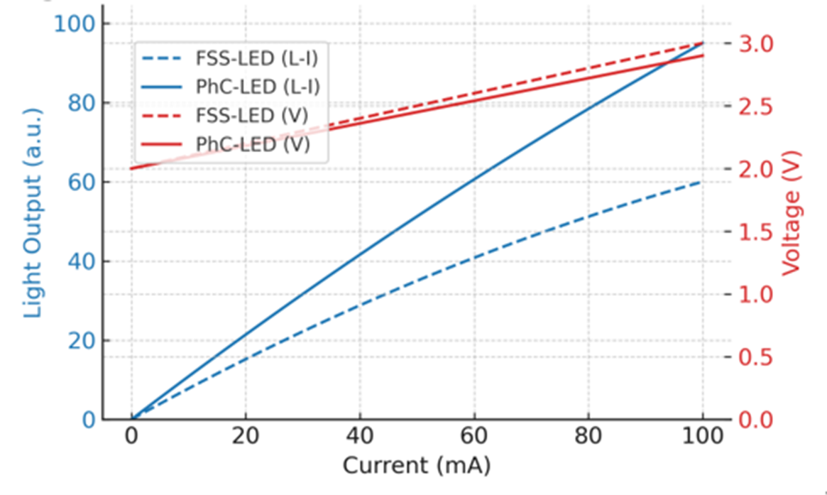
Figure 13. Typical L–I–V characteristics of conventional GaN-based LED and GaN-based LED with photonic crystal (PhC) structures[80].
As shown in Figure 13, GaN-based LEDs with photonic crystal (PhC) structures exhibit superior light intensity and electrical performance compared to conventional structures. Furthermore, studies have demonstrated that forming a two-dimensional porous array in the p-GaN layer of ultraviolet LEDs not only enhances light extraction but also improves current spreading[80]. The introduction of porous sidewalls helps to reduce electrode shadowing and absorption losses, thereby improving the light output efficiency of deep-UV chips without compromising their compact dimensions[81,83].In addition, the mechanical compliance of porous GaN makes it highly suitable for strain engineering and microstructural modulation. For example, integrating a compressible porous GaN buffer layer beneath a micro-LED array can alleviate substrate-induced stress and enable pixel-level strain tuning, allowing for precise control of emission wavelengths[85]. Inspired by this concept, the UCSB research team successfully utilized porous GaN to relax strain in regrown InGaN layers on micron-scale nitride LEDs, expanding the emission range into the green and even orange spectral regions[86]. This indicates that in deep-UV LEDs, porous interlayers may also be employed to relieve strain, improve crystal quality, and thereby indirectly enhance emission intensity[87,88].Beyond tuning intrinsic material properties, porous GaN can also serve as a three-dimensional scaffold for integrating other functional materials[89,90]. For instance, in recent studies on porous GaN for color-conversion displays, quantum dot (QD) solutions were infused into the porous network to form highly uniform QD/GaN composite structures[91,92] . This nanoporosity-enabled embedding approach significantly improves the QD fill factor and operational stability within LED pixels[93]. A similar concept can be applied to UV LEDs, where dielectric phosphors or dopants are incorporated into porous GaN to form composite emission layers or enhance p-type doping efficiency—an approach already considered feasible[94,95].
In summary, porous GaN offers new degrees of freedom for modulating both the optical field and material distribution at the microscale, thereby advancing functional integration in next-generation optoelectronic devices[96].
4.2. Application of Porous GaN in Full-Color Micro-LED Displays
With the rapid development of microdisplays and wearable electronics, micron-scale light-emitting diodes (Micro-LEDs) have garnered extensive attention in the field of full-color displays. However, one of the major challenges in Micro-LED technology lies in the monolithic integration of red, green, and blue (RGB) emitters on a single substrate. In this regard, porous GaN exhibits unique advantages by enabling stress engineering and wavelength tuning within a single material system, thus facilitating multicolor emission from a unified GaN platform[23,97].On one hand, the introduction of ordered porous structures into GaN substrates forms a “compliant” or “relaxed” template that can significantly reduce epitaxial stress. This permits the growth of high-indium-content InGaN emission layers without cracking, thereby extending the emission wavelength of InGaN into the green and even red spectral regions. Pasayat et al. reported a wavelength-tunable emission strategy utilizing porous GaN: electrochemical etching was performed on patterned GaN substrates to form porous templates with tailored porosity, followed by epitaxial growth of micron-scale InGaN emitters[97]. Compared to untreated samples, porous GaN-based Micro-LEDs exhibited a significant redshift in emission wavelength, indicating effective stress relaxation, enhanced indium incorporation, and extended wavelength emission[23]. The same group also successfully fabricated porous pseudo-substrates of high-indium-content AlGaN and InGaN, offering new avenues for red and deep-UV LED epitaxy.On the other hand, companies such as Porotech have developed a “dynamic pixel tuning” approach that incorporates nanoscale porosity into GaN emitter pixels. By modulating the drive current, single Micro-LED pixels can switch emission across blue, green, and red spectral bands[97]. Based on this porous GaN platform, researchers have demonstrated the world’s first full-color microdisplay using a single GaN wafer to achieve tunable RGB emission[6]. This monolithic full-color strategy eliminates the need for conventional mass transfer of RGB Micro-LEDs and is considered a breakthrough for high-resolution Micro-LED display technologies.
In addition to direct wavelength tuning, porous GaN also serves as an ideal host for integrating color conversion materials and improving optical output. Recent studies have demonstrated a technique for embedding quantum dot (QD) emitters within nanoporous GaN layers formed on the surface of InGaN-based Micro-LEDs[7]. The process involves UV-induced photoelectrochemical etching to generate nanostructured pores, which are subsequently filled with red and green QD phosphors. The resulting on-wafer integrated QD-conversion layers exhibit excellent color uniformity and over 90% color conversion efficiency, attributed to the mechanical confinement and homogeneous distribution offered by the porous GaN framework[98]. This embedded QD strategy combines the advantages of self-emission and color conversion, pushing the performance boundaries of high-brightness and wide-color-gamut Micro-LED displays. Porous GaN also improves light extraction in Micro-LEDs by mitigating optical confinement at the microscale. Its scattering properties alleviate the optical trapping typically observed in micron-scale pixels. Thaalbi et al. fabricated a periodic array of nanoporous GaN pyramids as light extraction layers for InGaN/GaN quantum wells, resulting in significantly enhanced emission intensity. This was considered a promising high-brightness solution beyond conventional planar Micro-LED architectures[98].Additionally, integrating porous distributed Bragg reflectors (DBRs) within Micro-LED pixels has been shown to further boost light output. Jarman et al. reported the fabrication of a high-reflectivity porous GaN/air DBR structure on a GaN substrate, followed by the epitaxial growth of InGaN Micro-LED arrays. The devices exhibited more than 50% improvement in light extraction efficiency compared to those grown on standard GaN substrates[99,100]. Similarly, Zhong et al. enhanced internal photon recycling by introducing a porous GaN reflector beneath InGaN quantum wells, significantly increasing emission intensity. These studies collectively demonstrate that porous GaN not only addresses the RGB integration challenge in Micro-LEDs, but also improves display performance through optical and structural engineering[101]. Currently, the application of porous GaN in Micro-LEDs is transitioning from laboratory research to industrial implementation[102,103]. Figure 14 illustrates the fabrication process of nanoporous GaN (NP-GaN) embedded with quantum dots for full-color Micro-LED displays. Such devices are beginning to show immense potential in next-generation microdisplay technologies.
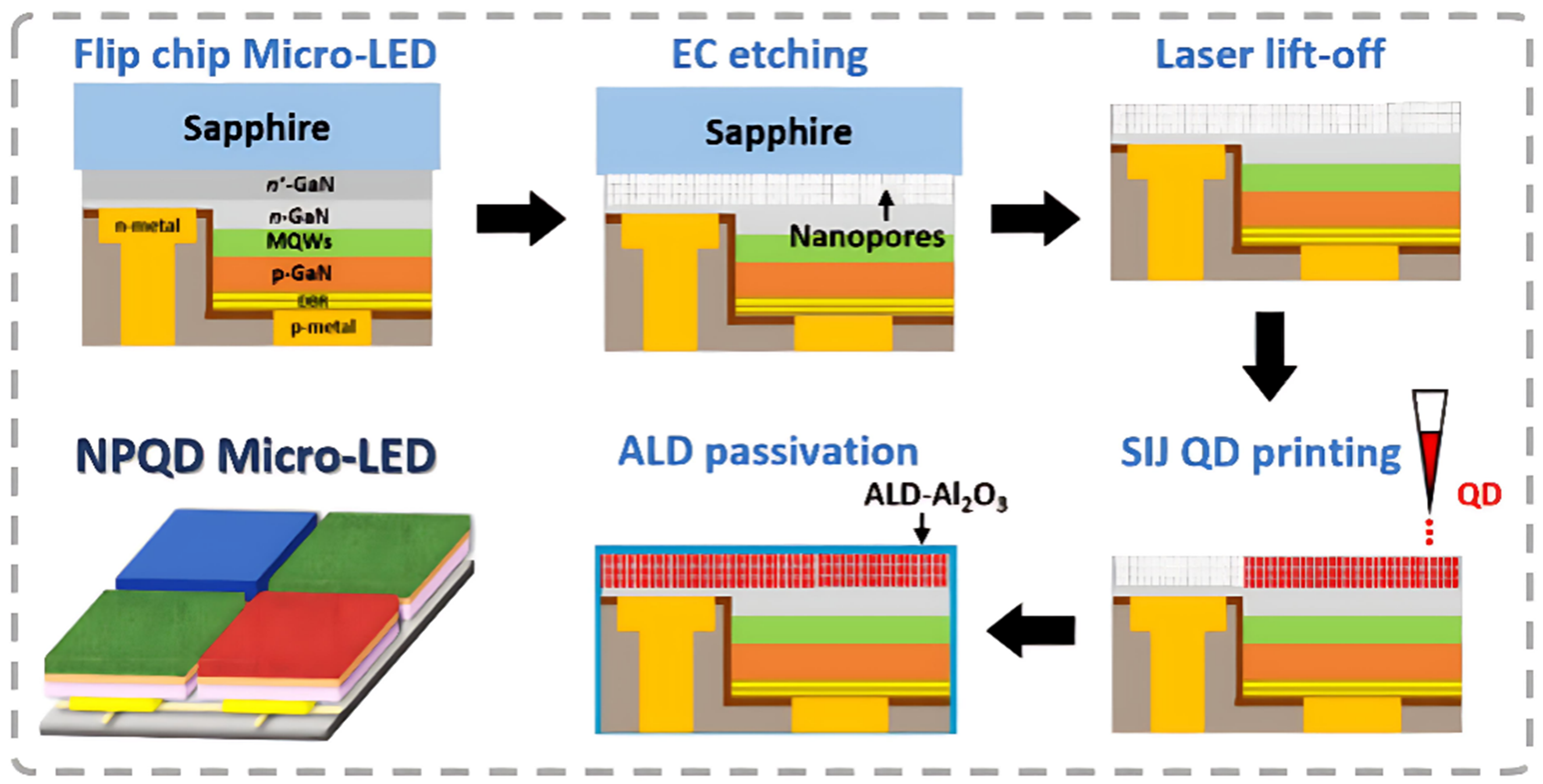
Figure 14. Fabrication process of nanoporous GaN (NP-GaN) embedded with quantum dots (QDs) for Micro-LED devices[92].
4.3. Application of Porous GaN in Ultraviolet Photodetectors
In addition to its important role in light-emitting devices, porous GaN also shows great potential for enhancing the performance of ultraviolet (UV) photodetectors[103,104] .GaN-based UV photodetectors, including photodiodes and photoconductive-type devices, require high optical absorption and efficient collection of photogenerated carriers. The incorporation of porous structures offers advantages in increasing the light-absorbing surface area, reducing reflectivity, and modulating carrier recombination dynamics[92,105].Yu et al. fabricated a metal–semiconductor–metal (MSM) deep-UV photodetector based on porous GaN thin films and observed a substantial enhancement in photoresponsivity to near-UV light (~360 nm), approximately doubling the response compared to planar GaN-based detectors[98]. This performance improvement was attributed to the higher specific surface area and enhanced multiple scattering within the porous structure, which extended the effective optical path length in the semiconductor and facilitated increased carrier generation[99,85].However, porous architectures can also introduce surface state traps, which may elevate dark current levels and slow response times in photodetectors. To address these issues, researchers have proposed incorporating wide-bandgap insulators or heterojunctions into the porous GaN structure to passivate traps and suppress leakage currents. Wen et al. designed a Ga₂O₃/porous GaN composite photodetector, in which a porous GaN distributed Bragg reflector (DBR) served as a UV-reflecting buffer layer and a single-crystalline Ga₂O₃ overlayer acted as a passivation layer. Experimental results demonstrated that, compared to devices using porous GaN alone, this heterostructure exhibited a photo-to-dark current ratio improvement of over two orders of magnitude under 365 nm illumination, with a detectivity of 8.9 × 10¹⁰ Jones and faster photoresponse rise/fall times of 0.33/0.23 s, respectively. The improvement was attributed to the Ga₂O₃ layer effectively blocking surface leakage pathways and suppressing trap-assisted recombination in porous GaN.In another study, demonstrated a self-powered UV detector by transferring a graphene layer onto porous GaN to form a heterojunction. In this configuration, porous n-GaN and p-type organic semiconductors (e.g., copper phthalocyanine) formed a heterojunction photodiode that generated a measurable photocurrent without external bias. The device exhibited an on/off current ratio exceeding 10³ and showed good spectral selectivity[102].These findings suggest that structural hybridization and interface engineering can effectively mitigate key performance bottlenecks in porous GaN-based UV photodetectors, such as high dark current and slow response times. As shown in Figure 15, the I–V characteristics under 365 nm UV illumination clearly demonstrate a distinct contrast between dark and photocurrent, highlighting the stability and sensitivity of the device[102,103].
Looking forward, combining porous GaN with other wide-bandgap semiconductors (such as oxides and nitrides) to construct novel heterojunction photodetectors, as well as engineering porous structure arrays to enhance light coupling, represent promising strategies for advancing UV detection technologies.
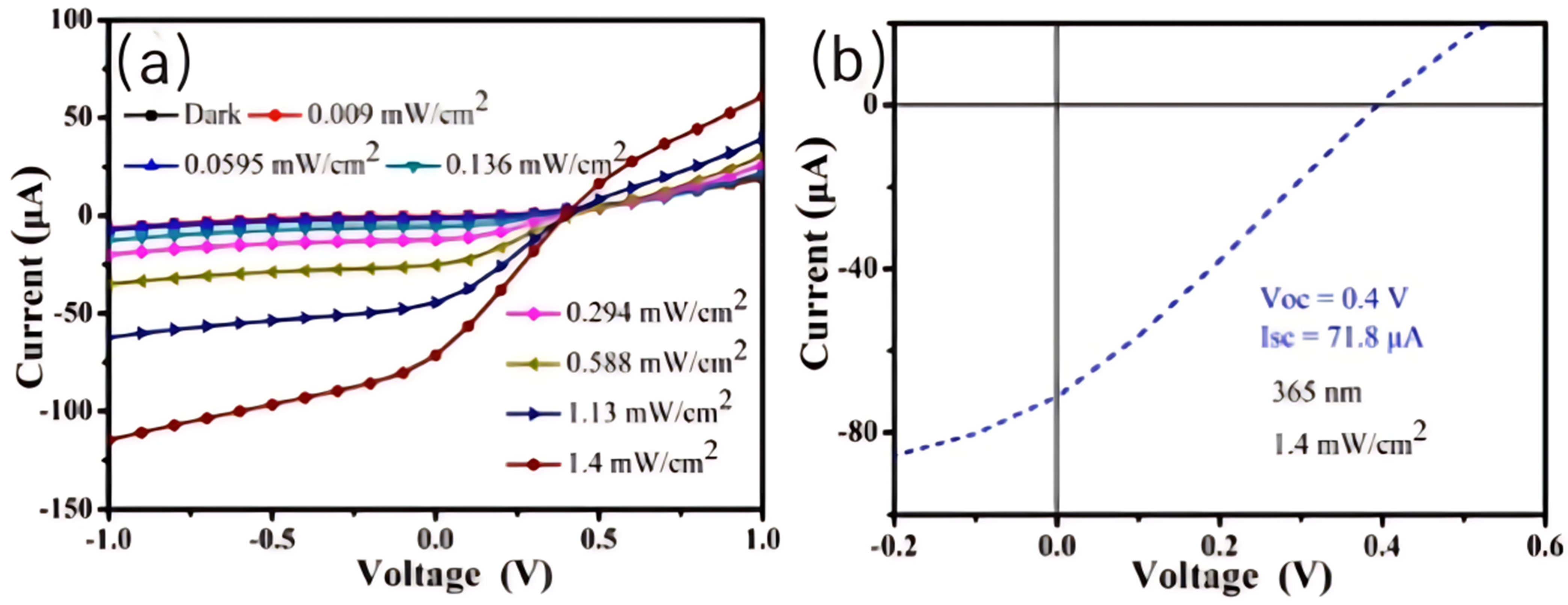
Figure 15. (a) Current–voltage (I–V) curves of the photodetector (PD) under 365 nm light with di erent powerdensities from 0to1.4mWcm-2 illumination. (b)Photovoltaice ectofthecorrespondingdevice[102].
4.4 .Application of Porous GaN in Photonic Crystals and Optical Resonator Devices
The tunable refractive index enabled by porous GaN makes it an ideal building block for photonic crystal structures and optical resonator devices[104]. Conventional GaN-based photonic components—such as vertical-cavity surface-emitting lasers (VCSELs) and resonant-cavity light-emitting diodes (RCLEDs)—often require the integration of high-reflectivity distributed Bragg reflectors (DBRs) within the nitride epitaxial structure[92,105]. However, due to the limited refractive index contrast between GaN and typical dielectric materials, traditional all-solid GaN/AlGaN DBRs demand several tens of mirror pairs to achieve sufficient reflectivity, significantly complicating the epitaxial process. The introduction of porous structures offers a solution to this challenge. Zhang et al. fabricated highly porous GaN/air multilayers and experimentally demonstrated that only ~10 pairs of layers were sufficient to achieve broadband reflectivity exceeding 99%.This work was the first to explicitly apply porous nitride films for photonic engineering, highlighting the powerful capability of porosification to modulate the effective dielectric constants of semiconductor materials[67].Subsequently, Lee et al. successfully integrated porous GaN DBRs into GaN-based VCSELs, achieving ultraviolet lasing under optical pumping conditions. Compared to conventional DBRs formed by stacking oxide mirrors, porous GaN DBRs enable monolithic nitride-based resonant cavities with superior thermal expansion matching and improved process compatibility.
Further advances led to the realization of electrically driven resonant-cavity LEDs. Mishkat-Ul-Masabih et al. fabricated a cavity LED structure on m-plane GaN incorporating a bottom porous GaN/air DBR and a top highly reflective metal mirror. The resulting electroluminescent device exhibited significant spectral narrowing and enhanced output intensity in specific cavity modes[106]. This demonstrated that porous GaN can not only serve as a passive photonic component but can also be integrated into active emission devices, enabling precise spectral and modal control.Figure 16, adapted from Zhang et al. (ACS Photonics, 2015), presents the experimental and simulated reflectance spectra of alternating GaN/NP-GaN DBR structures, showing a peak reflectivity greater than 99.5%[107].
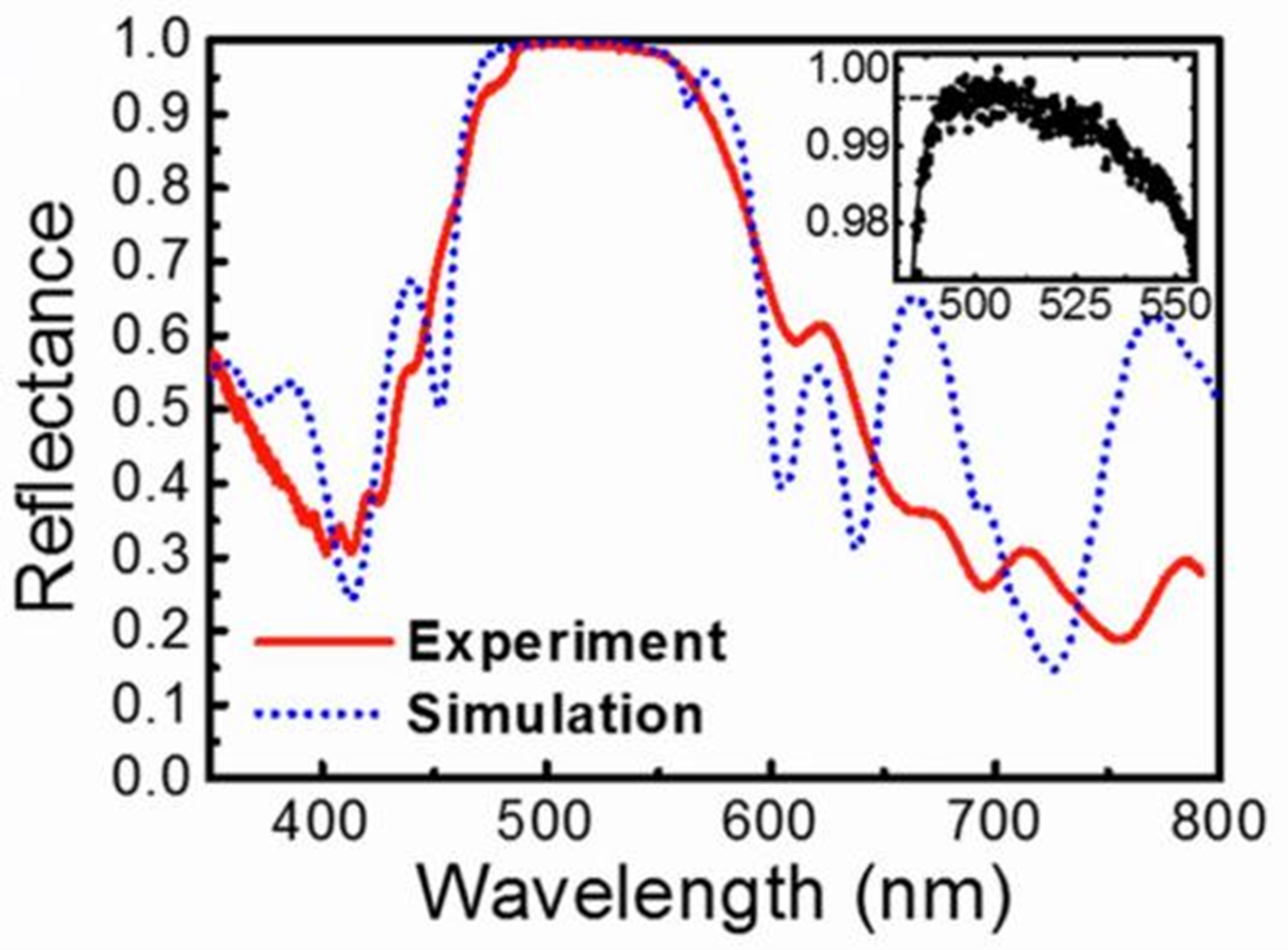
Figure 16. Experimentally measured (red solid line) and COMSOL-simulated (blue dotted line) reflectance spectra from a DBR region. Inset: close-up of a reflectance spectrum (dots, experimental data; line, fit to the data) with a peak reflectance exceeding 99.5%[107].
In addition to its use in conventional optical cavities, the intrinsic anisotropic structures within porous GaN impart unique optical properties such as birefringence and directional reflectivity. During electrochemical etching along the c-axis of GaN, differences in surface polarity enable the formation of vertically aligned nanopore arrays, resulting in dielectric anisotropy[108]. ElAfandy et al. reported that a 5 μm-thick oriented porous GaN layer exhibited a birefringence index difference of approximately 0.06—an effect not attainable in conventional isotropic GaN crystals[108]. This engineered birefringence opens new possibilities for integrating GaN-based waveplates and polarization elements, expanding its functionality in optical signal manipulation. Similarly, by precisely controlling the geometry and periodicity of the porous structure, it is possible to design two- and three-dimensional photonic crystals (PhCs) with customized photonic bandgap properties. Under appropriate conditions, porous GaN can form a fully interconnected 3D network that exhibits photonic bandgap behavior at specific wavelengths. Although the fabrication of complete photonic crystal structures in GaN remains challenging, porosification provides a promising bottom-up approach to constructing subwavelength periodic architectures.
The application of porous GaN in short-wavelength laser sources has also attracted increasing attention. Deep-UV laser diodes are extremely sensitive to optical mode confinement and propagation loss. To address this, researchers have introduced porous GaN into the cladding layers of AlGaN laser structures to reduce mode refractive index and optimize field distribution. Recently, Zhao et al. reported that integrating low-refractive-index nanoporous interlayers significantly enhanced the optical confinement factor and dramatically reduced the threshold current density—a key indicator of lasing efficiency[109,110]. This represents the first demonstration of porous GaN improving deep-UV laser performance and underscores its potential in future short-wavelength laser devices. Similarly, Wu et al. implemented porous AlGaN DBRs to enhance light extraction and in-cavity field intensity in deep-UV LEDs. This structure enabled spectral modulation and boosted emission efficiency[109]. In a recent review, Lim et al. further highlighted the prospective use of porous III-nitrides in edge-emitting lasers, microcavity lasers, and other photonic devices, where stress engineering combined with optical design could lead to enhanced performance[110,111]. To meet the demands of practical device integration, the fabrication of porous GaN optical structures is also advancing toward large-area scalability and precise control. Liu et al. achieved uniform fabrication of porous AlGaN DBRs on a 2-inch GaN wafer using a single-step wet etching process, with reflectance peaks tunable across the 250–290 nm range. This result demonstrates the feasibility of wafer-scale, high-uniformity porous GaN photonic crystals and mirrors, paving the way for their integration into large-scale optoelectronic systems[112,113].
5. Conclusion and Outlook
Porous GaN, as a new functional material, is pushing forward the development of bandgap semiconductor devices. It has made technical breakthroughs in many integration fields from the beginning to improve the efficiency of light extraction. It has shown great potential. The classical one is that the luminous efficiency and quality of ultraviolet LED devices have been obviously improved after GaN materials with porous structure are introduced. Some studies have shown that ultra-high light extraction gains of 50% can be achieved after introducing porous structures, and the effect is remarkable. In addition, porous GaN has unique advantages in emissivity regulation, stress release and structure integration. Researchers are constantly using the unique advantages of porous GaN to expand application fields. For example, some teams have realized Micro-LED full-color display under a single material system[102], some teams have improved the working efficiency, sensitivity and stability of ultraviolet detectors, and the use of porous materials as buffer layers can effectively reduce defect density and improve device reliability [92,114].With the gradual improvement of understanding of physical mechanisms and the maturity of wafer-level porous processe[115]. Porous GaN will play a more important role in the next generation of optoelectronic devices, but even though porous materials have their unique advantages, there are still some problems to be solved. The influence mechanism of various factors such as topography and size of porous structure on the comprehensive performance of devices still needs more in-depth study[116,117]. In addition, the optimization standards of porous size and density are different in different application scenarios. How to reasonably control the parameters of porous materials according to different application scenarios to achieve the best performance of devices is an important topic for researchers to study at presen[70,118].Simultaneously, researchers must address critical challenges including the potential changes in stability and reliability of porous GaN devices during long-term operation, the impact of packaging processes on the porous layer [114], and the structural/functional stability of the porous system under cyclic thermal stress. Resolving these issues demands extensive rigorous research and experimental validation. It has been found that when porous structures are applied to high power devices, their thermal conductivity will decrease, and high thermal conductivity filling materials may be needed to compensate for this. Recent studies have shown that the thermal conductivity of porous GaN can decrease from approximately 130 W/m·K to about 10 W/m·K due to increased porosity, which is beneficial for on-chip thermal insulation but may pose challenges for heat dissipation in high-power devices[119]. To address these challenges, innovative packaging solutions have been explored. For instance, the MORGaN project developed advanced 3D ceramic packaging and new metallization techniques using MN+1AXN alloys to ensure thermal compatibility and chemical stability in extreme conditions[120]. Additionally, integrating porous GaN with high thermal conductivity materials, such as diamond substrates, has demonstrated improved thermal management. A simulation study indicated that transferring GaN HEMTs to diamond substrates reduced lattice temperatures from 507 K to 372 K and decreased total thermal resistance by a factor of five[121]. Researchers are also actively looking for new ways to solve the problem. For example, the combination of material and structure design (such as energy band engineering superimposed porous optical engineering) can be regarded as a new direction to improve the efficiency of ultraviolet LED. At the same time, porous GaN also plays its own unique advantages in ultraviolet detectors, single photon detectors and many other fields. Amano et al. look forward to the development trend of AlGaN based deep ultraviolet LED/laser, and think that porous structure will become the key to realize high efficiency deep ultraviolet light source[119].
In summary, with sustained advancements in porous material research, porous GaN has evolved far beyond its original role as a light extraction enhancer. It now represents a multifunctional platform that drives innovation across a wide spectrum of optoelectronic devices. This review has comprehensively demonstrated how porous GaN improves light output through refractive index modulation, scattering enhancement, critical angle expansion, and distributed Bragg reflector (DBR) integration. Furthermore, its ability to simultaneously relieve stress, passivate defects, and enable integration with diverse material systems highlights its unparalleled versatility. Notably, porous GaN has been successfully applied in ultraviolet LEDs, Micro-LED displays, UV photodetectors, and photonic resonators, enabling improvements in quantum efficiency, wavelength tuning, emission directionality, and integration density. These achievements underscore the transition of porous GaN from a passive enhancement layer to an active component in device-level engineering. Looking forward, future research is expected to further exploit the unique properties of porous GaN through interdisciplinary integration. Promising directions include the creation of novel heterostructures via organic or 2D materials, incorporation of phase-change and high thermal conductivity materials for thermal management, and exploration of its role in quantum devices and bio-optoelectronic systems[122]. As fabrication techniques mature and understanding deepens, porous GaN is poised to enable high-efficiency deep UV LED arrays, integrated photonic circuits, and flexible ultraviolet photovoltaic platforms—accelerating the journey from laboratory-scale demonstrations to real-world technological breakthroughs.
Conflicts of Interest
The authors declare no conflict of interest.
Acknowledgements
The authors would like to extend their heartfelt gratitude to Mr. Jianfei Li and Professor Jiancai Leng for their patient guidance, insightful feedback, and unwavering support throughout the course of this research. Their profound knowledge and meticulous instruction in GaN-based optoelectronic materials and devices have played a pivotal role in shaping the quality and direction of this work. The authors also gratefully acknowledge the contributions of their research group members and technical staff, whose assistance in experimental analysis and data processing greatly facilitated this study. Finally, the authors express sincere appreciation to all dedicated researchers working tirelessly in this field. It is through their continued innovation and perseverance that the present work could be built upon a solid and evolving foundation of knowledge.
References
-
R. K. Mondal, H. Alrowaily, A. A. Ansari, S. M. Alshehri, A. S. Aldwayyan. “Recent advances and challenges in AlGaN-based ultra-violet light emitting diode technologies.” Mater. Res. Bull. 2021, 140, 111258.
-
Y. Nagasawa, A. Hirano. “Review of encapsulation materials for AlGaN-based deep-ultraviolet light-emitting diodes.” Photonics Res. 2019, 7, 8, B55–B65.
-
J. Park, J. H. Kang, S. W. Ryu. “High diffuse reflectivity of nanoporous GaN distributed Bragg reflector formed by electrochemical etching.” Appl. Phys. Express 2013, 6, 7, 072201.
-
C. Zhang, S. H. Park, D. Chen, D. W. Lin, W. Xiong, H. C. Kuo, C. F. Lin, H.Cao, J. Han. “Mesoporous GaN for photonic engineering – highly reflective GaN mirrors as an example.” ACS Photonics 2015, 2, 7, 980–986.
-
S. M. Lee, S. H. Gong, J. H. Kang, M. Ebaid, S. W. Ryu, Y. H. Cho. “Optically pumped GaN vertical cavity surface emitting laser with high index-contrast nanoporous distributed Bragg reflector.” Opt. Express 2015, 23, 9, 11023–11030.
-
G. Y. Shiu, K. T. Chen, F. H. Fan, K. P. Huang, W. J. Hsu, J. J. Dai, C. F. Lai, C. F. Lin. “InGaN light-emitting diodes with an embedded nanoporous GaN distributed Bragg reflectors.” Sci. Rep. 2016, 6, 29138.
-
F. H. Fan, Z. Y. Syu, C. J. Wu, Z. J. Yang, B. S. Huang, G. J. Wang, Y. S. Lin, H. Chen, C. H. Kao, C. F. Lin. “Ultraviolet GaN light-emitting diodes with porous-AlGaN reflectors.” Sci. Rep. 2017, 7, 4968.
-
G. J. Wang, B. S. Hong, Y. Y. Chen, Z. J. Yang, T. L. Tsai, Y. S. Lin, C. F. Lin. “GaN/AlGaN ultraviolet light-emitting diode with an embedded porous-AlGaN distributed Bragg Reflector.” Appl. Phys. Express 2017, 10, 12, 122102.
-
X. D. Lu, J. Li, K. Su, C. Ge, Z. C. Li, T. Zhan, G. H. Wang, J. M. Li. “Performance-Enhanced 365 nm UV LEDs with Electrochemically Etched Nanoporous AlGaN Distributed Bragg Reflectors.” Nanomaterials 2019, 9, 6, 862.
-
G. Yuan, C. Zhang, K. Xiong, J. Han. “InGaN/GaN microdisks enabled by nanoporous GaN cladding.” Opt. Lett. 2018, 43, 22, 5567–5570.
-
S. Ding, Y. W. Li, X. Q. Xiu, X. M. Hua, Z. L. Xie, T. Tao, P. Chen, B. Liu, R. Zhang, Y. D. Zheng. “Comparison study of GaN films grown on porous and planar GaN templates.” Chin. Phys. B 2020, 29, 3, 038103.
-
H. Y. Hsieh, P. W. Liou, S. Yang, W. C. Chen, L. P. Liang, Y. C. Lee, C. C. Yang. “Behaviors of AlGaN strain relaxation on a GaN porous structure studied with d-spacing crystal lattice analysis.” Nanomaterials 2023, 13, 10, 1617.
-
C. Wurm, H. Collins, N. Hatui, W. Li, S. Pasayat, R. Hamwey, K. Sun, I. Sayed, K. Khan, E. Ahmadi, S. Keller, U. Mishra. “Demonstration of device-quality 60% relaxed In₀.₂Ga₀.₈N on porous GaN pseudo-substrates grown by PAMBE.” Appl. Phys. Lett. 2022, 120, 1, 012101.
-
M. E. Raypah, A. A. Ahmed, A. F. Omar. “Application of porous materials and structures for improving optical and thermal performance of inorganic and organic light-emitting diodes: A review.”Sensors Actuators A Phys. 2022, 347, 113966.
-
F. C.-P. Massabuau, P. H. Griffin, H. P. Springbett, Y. Liu, R. V. Kumar, T. Zhu, R. A. Oliver. “Dislocations as channels for the fabrication of sub-surface porous GaN by electrochemical etching.” APL Mater. 2020, 8, 3, 031115.
-
H. Hartono, C. B. Soh, S. Y. Chow, S. J. Chua, E. A. Fitzgerald “Reduction of threading dislocation density in GaN grown on strain-relaxed nanoporous GaN template.” Appl. Phys. Lett. 2007, 90, 17, 171917.
-
P. H. Griffin, M. Frentrup, T. Zhu, M. E. Vickers, R. A. Oliver. “Structural characterization of porous GaN distributed Bragg reflectors using x-ray diffraction.” J. Appl. Phys. 2019, 126, 21, 213109.
-
R. Butté, E. Feltin, J. Dorsaz, G. Christmann, J.-F. Carlin, N. Grandjean, M. Ilegems. “Recent progress in the growth of highly reflective nitride-based distributed Bragg reflectors and their use in microcavities.” Jpn. J. Appl. Phys. 2005, 44, 10, 7207–7216.
-
X. Liu, Z. X, Lv, Z. F. Liao, Y. C. Sun, Z. Q. Zhang, K. Sun, Q. X. Zhou, B. Tang, H. S. Geng, S. L. Qi, S. J. Zhou. “Highly efficient AlGaN deep-ultraviolet LEDs by bandgap and device structure engineering.” Microsyst. Nanoeng. 2024, 10, 110.
-
L. F. He, W. Zhao, K. Zhang, C. G. He, H. L. Wu, N. Y. Liu, W. D. Song, Z. T. Chen, S. T. Li. “Performance enhancement of AlGaN-based 365 nm ultraviolet light-emitting diodes with a band-engineering last quantum barrier.” Opt. Lett. 2018, 43, 3, 515–518.
-
Y. S. Lin, M. Y. Chen, T. Y. Chen, C. J. Huang. “Multiple fields manipulation on nitride material structures in ultraviolet light-emitting diodes.” Sci. Rep. 2021, 11, 13078.
-
M. A. Khan, N. Maeda, J. Yun, M. Jo, Y. Yamada, H. Hirayama. “Achieving 9.6% efficiency in 304 nm p-AlGaN UVB LED via increasing the hole injection and light reflectance.” Photonics Res. 2022, 12, 9, 2591.
-
M. Kneissl, T.-Y. Seong, J. Han, H. Amano. “The emergence and prospects of deep-ultraviolet light-emitting diode technologies.” Nat. Photonics 2019, 13, 4, 233–244.
-
J. Liu, J. Cui, H. Xiao. “Electrochemical etching of n-type GaN in different electrolytes.” J. Alloys Compd. 2024, 983, 167054.
-
J. Cui, H. Chen, F. Yang, H. Xiao. “Fabrication of InGaN/GaN multiple quantum well embedded on nanoporous GaN mirror under different acid electrolytes.” Opt. Mater. 2023, 145, 114469.
-
H. Amano, H. Hirayama, Y. Tsuda, Y. Kawaguchi. “Prospects and development of AlGaN-based deep-UV LEDs for disinfection.” J. Phys. D: Appl. Phys. 2020, 53, 50, 503001.
-
J. Jarman, H. Kim, B. Lee, S. Nakamura. “Light-output enhancement of InGaN LEDs regrown on nanoporous GaN DBR substrates.” Proc. SPIE 2019, 10918, 109180T.
-
T. Zhu, Y. Liu, T. Ding, W. Y. Fu, J. Jarman, C. X. Ren, R. V. Kumar, R. A. Oliver. “Wafer-scale Fabrication of Non-Polar Mesoporous GaN Distributed Bragg Reflectors via Electrochemical Porosification.” Sci. Rep. 2017, 7, 45344.
-
R. T. ElAfandy, A. K. Mohd, N. H. Awang. “Optical anisotropy in porous GaN: enhanced birefringence for photonic applications.” Appl. Phys. Lett. 2021, 118, 22, 221901.
-
J. T. Griffiths, M. J. Davies, T. Wilson. “Porous gallium nitride: from strain engineering to new device opportunities.” Phys. Status Solidi A 2020, 217, 1, 1900825.
-
Z. Hou, F. Zhang, P. Chen, X. Yang. “Research progress of AlGaN-based deep UV-LEDs. ” Crystals 2022, 12, 7, 950.
-
M. Kneissl, J. Rass, III-Nitride Ultraviolet Emitters: Technology and Applications, Springer, Cham 2016.
-
L. Zhang, W. Tang, J. Li. “High-efficiency deep-ultraviolet light-emitting diodes.” Light Sci. Appl. 2022, 11, 26.
-
S. J. Park, H. Kim, T. Y. Seong. “Recent progress in high-efficiency UV LEDs: device structure and packaging.” IEEE J. Sel. Top. Quantum Electron. 2020, 26, 1, 1601620.
-
Y. M. Zhao, M. C. Shan, Z. H. Zheng, P. C. Jian,W. J. Liu,S .Z. Tan,C. Q. Chen, F. Wu,J N.Dai.“Wafer-scale nanoporous AlGaN-based DUV DBRs via one-step wet etching.” Sci. Rep. 2022, 12, 22434.
-
A. Shushanian, D. Iida, Z. Zhuang, Y. Han, K. Ohkawa. “Electrochemical etching mechanism in oxalic acid for porous GaN.” RSC Adv. 2022, 12, 8, 4648–4655.
-
A. H. Park, S. Baek, Y. W. Kim, S. Chandramohan, E. K. Suh, T. H. Seo. “Defect-selective-etched porous GaN as a buffer layer for high efficiency InGaN/GaN light-emitting diodes.” PLOS One 2022, 17, 11, e0277667.
-
R. Zhang, H. Zhang, Y. Sakai, K. Tanaka. “Nanoporous AlGaN distributed Bragg reflectors for deep UV emission.” ACS Appl. Nano Mater. 2022, 5, 7, 10081–10089.
-
X. D. Lu, J. Li, K. Su, C. Ge, Z. C. Li, T. Zhan, G. H. Wang, J. M. Li. “Enhanced 365 nm UV LEDs with nanoporous AlGaN DBRs.” Nanomaterials 2019, 9, 6, 862.
-
Y. F. Li, C. Y. Wang, Y. Zhang, P. Hu, S. N. Zhang, M. Q. Du, X. L. Su, Q. Li, F. Yun. “Analysis of TM/TE mode enhancement and droop reduction by a nanoporous n-AlGaN underlayer in a 290 nm UV-LED.” Photonics Res. 2020, 8, 6, 806–811.
-
Y. M. Zhao, L. Q. Deng, F. Wu, Z. H. Zheng, P. C. Jian, W. J. Liu, Z. Y. Chen, S. Z. Tan, M. Peng, W. Guo, C. Q. Chen, J. N. Dai. “Low-threshold AlGaN-based deep ultraviolet laser enabled by a nanoporous cladding layer.” Opt. Lett. 2024, 49, 4, 1061–1064.
-
D. Zhuang, J. H. Edgar. “Wet etching of GaN, AlN, and SiC: a review.” Mater. Sci. Eng. R: Rep. 2005, 48, 1, 1–46.
-
D. T. Chen, H. D. Xiao, J. Han. “Nanopores in GaN by electrochemical anodization in hydrofluoric acid: formation and mechanism.” J. Appl. Phys. 2012, 112, 6, 064303.
-
E. Monaico, C. Moise, G. Mihai, V. V. Ursaki, K. Leistner, I. M. Tiginyanu, M. Enachescu, K. Nielsch. “Towards uniform electrochemical porosification of bulk HVPE-grown GaN.” J. Electrochem. Soc. 2019, 166, 5, H3159–H3166.
-
O. Ambacher. “Growth and applications of Group III-nitrides.” J. Phys. D: Appl. Phys. 1998, 31, 20, 2653–2710.
-
R. F. Radzali, M. A. Mahdi, S. Shafie. “Characteristics of porous GaN prepared by KOH photoelectrochemical etching.” Mater. Res. Innov. 2014, 18, 6, 412–416.
-
M. J. Schwab, C. J. Kersten, M. Mastro. “Aligned mesopore arrays in GaN by anodic etching and photoelectrochemical surface etching.” J. Phys. Chem. C 2013, 117, 33, 16890–16895.
-
C. Youtsey, I. Adesida, G. Bulman. “Highly anisotropic photoenhanced wet etching of n-type GaN.” Appl. Phys. Lett. 1997, 71, 15, 2151–2153.
-
S. S. Pasayat, C. Gupta, Y. F. Wang, S. P. DenBaars, S. Nakamura, S. Keller, U. K. Mishra. “Compliant micron-sized patterned InGaN pseudo-substrates utilizing porous GaN.” Materials 2020, 13, 1, 213.
-
M. Okuda, K. Ueno, A. Itoh. “Porous GaN as a template to produce surface-enhanced Raman scattering substrates.” Appl. Phys. Lett. 2003, 83, 22, 4656–4658.
-
H. Watanabe, S. Nakamura, Y. Ueno. “Fabrication of porous GaN using Pt-assisted electrochemical etching and its application to light emitting devices.” Phys. Status Solidi C 2008, 5, 6, 1905–1907.
-
C. Yang, X. Xi, Z. G. Yu, H. C. Cao, J. Li, S. Lin, Z. H. Ma, L. X. Zhao. “Light modulation and water splitting enhancement using a composite porous GaN structure.” ACS Appl. Mater. Interfaces 2018, 10, 6, 5492–5497.
-
Y. H. Lee, J. H. Kang, S. W. Ryu. “Enhanced photocurrent and persistent photoconductivity in nanoporous GaN formed by electrochemical etching.” Thin Solid Films 2013, 540, 150–154.
-
S. F. Cheah, S. S. Ng, F. K. Yam, A. B. Hamid. “Formation and optical studies of porous GaN thin films via UV-assisted electrochemical etching approach.” Adv. Mater. Res. 2014, 895, 45–50.
-
Y. Kumazaki, S. Matsumoto, T. Sato. “Precise structural control of GaN porous nanostructures utilizing anisotropic electrochemical and chemical etching for the optical and photoelectrochemical applications.” J. Electrochem. Soc. 2017, 164, 7, H477–H483.
-
M. Manfang, L. Du, G. Liu, C. Zhu. “Research on micro-nanofabrication of GaN based on photoelectrochemical etching.” J. Foshan Univ. (Nat. Sci. Ed.) 2022, 40, 1, 59–64.
-
M. R. Zhang, S. J. Qin, H. D. Peng, G. B. Pan. “Porous GaN photoelectrode fabricated by photo-assisted electrochemical etching using ionic liquid as etchant.” Mater. Lett. 2016, 182, 363–366.
-
J. H. Kang, M. Ebaid, J. K. Lee, T. Y. Jeong, S. W. Ryu. “Vertical LED via thermal deformation of nanoporous GaN.” ACS Appl. Mater. Interfaces 2014, 6, 11, 8683–8687.
-
B. C. Shieh, Y. C. Jhang, K. P. Huang, W. C. Huang, J. J. Dai, C. F. Lai, C. F. Lin. “InGaN light-emitting diodes with embedded nanoporous GaN distributed Bragg reflectors.” Appl. Phys. Express 2015, 8, 8, 082101.
-
C. B. Soh, C. B. Tay, R. J. N. Tan, A. P. Vajpeyi, I. P. Seetoh, K. K. Ansah-Antwi, S. J. Chua. “Nanopore morphology in porous GaN template and its effect on the LEDs emission.” J. Phys. D: Appl. Phys. 2013, 46, 36, 365102.
-
A. Shushanian, D. Iida, Z. Zhuang, Y. Han, K. Ohkawa. “Analysis of the n-GaN electrochemical etching process and its mechanism in oxalic acid.” RSC Adv. 2022, 12, 8, 4648–4655.
-
Y. P. Hong, J. H. Park, C. W. Park, H. M. Kim, D. K. Oh, B. G. Choi, S. K. Lee, K. B. Shim. “Investigation of defects and surface polarity in AlN and GaN using wet chemical etching technique.” J. Korean Phys. Soc. 2014, 24, 5, 196–201.
-
J. C. Jarman, T. Zhu, P. H. Griffin, R. A. Oliver. "Light-output enhancement of InGaN light emitting diodes regrown on nanoporous distributed Bragg reflector substrates" Jpn. J. Appl. Phys. 2019, 58, SC, SCCC14.
-
D. T. Chen,H. D. Xiao , J. Han “Nanopores in GaN by electrochemical anodization in hydrofluoric acid: Formation and mechanism” J. Appl. Phys. 2012, 112, 6, 064303.
-
S. Chandramohan, A. H. Park, S. Baek, H. J. Lee. “Air-voids embedded GaN: strain relaxation and light extraction in LEDs.” Appl. Phys. Lett. 2021, 119, 26263102.
-
H. Liu, Y. F. Li, S. Wang, Z. Q. Lin. “Air-void embedded GaN-based light-emitting diodes grown on laser drilling patterned sapphire substrates.” Appl. Phys. Lett. 2016, 109, 4, 041104.
-
J. C. Jarman, T. T. Zhu, P. H. Griffin, R. A. Oliver. “Light-output enhancement of InGaN light emitting diodes regrown on nanoporous distributed Bragg reflector substrates.” Jpn. J. Appl. Phys. 2019, 58, SC, SCCC14.
-
X. L. Zhong, S. J. Haigh, X. Zhou, P. J. Withers. “Porous-GaN mirror to enhance InGaN MQW emission.” Vacuum 2020, 182, 109669.
-
S. H. Seo, Y. H. Cho, J. H. Kang, T. K. Lee. “Nanoporous GaN buffer for AlGaN DUV LEDs.” Crystals 2022, 12, 12, 1812.
-
Z. Hou, F. Zhang, P. Chen, Y. Liu. “Review of AlGaN-based DUV-LEDs.” Crystals 2022, 12, 8,950.
-
M. Shan, C. Guo, Y. Zhao, Q. Chen, Y. Liu, Y. Li, Z. Lin, J. Dai, F. Wu, L. Deng, P. Jian, S. Tan. “Nanoporous AlGaN DBRs for DUV LEDs.” ACS Appl. Nano Mater. 2022, 5, 9, 10081–10089.
-
S. J. Park, H. Kim, T. Y. Seong. “Advances in high-efficiency UV LED packaging.” IEEE J. Sel. Top. Quantum Electron. 2020, 26, 1,1601620.
-
S. Zhou, S. Liu, III-Nitride LEDs: From UV to Green, Springer, Singapore 2023.
-
S. Jin, D. Li, J. Zhang. “Polarization control in DUV LEDs using nanoporous underlayers.” Opt. Express 2020, 28, 15, 22463–22474.
-
X. Gao, X. Wu, Y. Ren. “Surface roughness and scattering enhancement in UV LEDs.” IEEE Photonics Technol. Lett. 2021, 33, 3, 150–153.
-
Y. Zhou, S. Huang, J. Wang. “Thermal reliability of nanoporous GaN devices.” IEEE Electron Device Lett. 2021, 42, 5, 758–761.
-
D. H. Kim, H. J. Kim, J. H. Ryu. “Electrochemical etching of Al-rich AlGaN for nanoporous DBRs.” ACS Omega 2020, 5, 43, 27170–27177.
-
J. Song, M. Wu, Z. Yang. “Micro-LED integration with nanoporous GaN for full-color displays.” J. Microelectron. Manuf. 2021, 4, 2, 144–150.
-
J. H. Kang, B. Li, T. Zhao, M. A. Johar, Y. Zhang, Y. Zhang, J. Han. “RGB Arrays for Micro-LED Applications Using Nanoporous GaN Embedded with Quantum Dots.” ACS Appl Mater. Interfaces 2020, 12, 25, 28021–28027.
-
S. M. Yu, Y. J. Chan, Y. S. Cheng, Y. D. Chen, Y. C. Kao, K. T. Chen, H. Chen, Y. S. Lin, J. Han, C. F. Lin. “Enhanced light extraction and electrical properties in ultraviolet-C AlGaN LEDs with porous hole-array patterns.” ACS Appl. Electron. Mater. 2025, 7, 3, 286–291.
-
N. Fiuczek, M. Sawicka, A. Feduniewicz-Żmuda, M. Siekacz, M. Żak, K. Nowakowski-Szkudlarek, G. Muziol, P. Wolny, J. J. Kelly, C. Skierbiszewski. “Electrochemical etching of p-type GaN using a tunnel junction for efficient hole injection.” Acta Mater. 2022, 234, 15, 118018.
-
Y. Zhao, M. Shan, Z. Zheng, P. Jian, W. Liu, S. Tan, C. Chen, F. Wu, J. Dai. “Fabrication of wafer-scale nanoporous AlGaN-based deep ultraviolet distributed Bragg reflectors via one-step selective wet etching.” Sci. Rep. 2022, 12, 22434.
-
M. F. Ain, N. N. Shamsuri, H. S. Lim. “Improvement of porous GaN-based UV photodetector with graphene cladding.” Appl. Sci. 2021, 11, 22, 10833.
-
C. F. Lin, Y. T. Zhang, C. J. Wang, Y. Y. Chen, G. Y. Shiu, Y. Ke, J. Han. “InGaN resonant microcavity with n⁺-porous-GaN/p⁺-GaN tunneling junction,” IEEE Electron Device Lett. 2021, 42, 9, 1568–1571.
-
S. S. Pasayat, C. Gupta, M. S. Wong, Y. Wang, S. Nakamura, S. P. DenBaars, S. Keller, U. K. Mishra. “Color-tunable <10 μm Square InGaN Micro-LEDs on Compliant GaN-on-Porous-GaN Pseudo-Substrates” Appl. Phys. Lett. 2020, 117, 6, 061105.
-
S. S. Pasayat, N. Hatui, W. Y. Li, C. Gupta, S. Nakamura, S. P. DenBaars, S. Keller, U. K. Mishra “High-Al-content AlGaN pseudo-substrates by porosification for deep-UV devices.” Appl. Phys. Lett. 2020, 117, 6, 062102.
-
H. Thaalbi, B. Kim, A. Abdullah, M. A. Kulkarni, F. Tariq, H. U. Din, Y. H. Cho, S. W. Ryu. “Porous GaN nanopyramids: advancing beyond conventional nanostructures for high-brightness InGaN/GaN quantum wells emission.” Adv. Funct. Mater. 2024, 34, 41, 2406467.
-
L. Zhang, Y. N. Guo, J. C. Yan, Q. Q. Wu, X. C. Wei, J. X. Wang, J. M. Li. “Deep ultraviolet LEDs with improved performance via nanoporous AlGaN templates.” Opt. Express 2019, 27, 4, 4917–4926.
-
Z. Zhang, M. Kushimoto, T. Sakai, N. Sugiyama, L. J. Schowalter, C. Sasaoka, H. Amano. “A 271.8 nm Deep-Ultraviolet Laser Diode for Room Temperature Operation.” Appl. Phys. Express 2019, 12, 12, 124003.
-
S. M. Mishkat-Ul-Masabih, A. Hurtado, Y. Q. Sun. “Electrically Injected M-Plane GaN Resonant-Cavity Light-Emitting Diode with Nanoporous GaN Bottom DBR.” ECS J. Solid State Sci. Technol. 2019, 12, 12, 124003.
-
J. Song, J. Kang, J. Han. “Monolithic RGB micro-LEDs with quantum dots embedded in nanoporous GaN.” ACS Appl. Electron. Mater. 2021, 3, 3, 1477–1484.
-
Y. M. Huang, J. H. Chen, Y. H. Liou, K. James Singh, W. C. Tsai, J. Han, C. J. Lin, T. S. Kao, C. C. Lin, S. C. Chen, H. C. Kuo. “High-uniform and high-efficient color conversion nanoporous GaN-based micro-LED display with embedded quantum dots.” Nanomaterials 2021, 11, 10, 2696.
-
T. H. Ngo, B. Gil, T. V. Shubina, B. Damilano, S. Vezian, P. Valvin, J. Massies. “Enhanced excitonic emission efficiency in porous GaN.” Sci. Rep. 2018, 8, 15767.
-
R. Xu, Q. Kang, J. Zhang, M. H. Khan, F. Y. Fu, M. A. Ali, J. S. Chang, H. Y. Lin. “Research progress of AlGaN-based deep ultraviolet light-emitting diodes.” Micromachines 2023, 14, 4, 844.
-
T. C. Hsu, Y. T. Teng, Y. W. Yeh, X. Fan, K. H. Chu, S. H. Lin, K. K. Yeh, P. T. Lee, Y. Lin, Z. Chen, T. Wu, H. C. Kuo. “Perspectives on UVC LED: its progress and application.” Photonics 2021, 8, 6, 196.
-
P. H. Griffin, T. Zhu, R. A. Oliver. “Porous AlGaN-based ultraviolet distributed Bragg Reflectors.” Materials 2018, 11, 9, 1487.
-
L. Cai, J. Pan, Y. Zhao, J. Wang, S. Xiao. “Porous gallium nitride: from strain engineering to new device opportunities.” Phys. Status Solidi A 2020, 217, 1900825.
-
K. Zhang, Y. Zhang, X. Wang, T. Yan, Y. Jiang. “Analysis of TM/TE Mode Enhancement and Droop Reduction by a Thin AlN Interlayer in AlGaN-Based UVC LEDs” Photonics Res. 2020, 8, 6, 806–811.
-
I. Geijselaers, N. Vainorius, S. Lehmann, C. Pryor, K. A. Dick, M. E. Pistol. “Atomically sharp, crystal phase defined GaAs quantum dots.” Appl. Phys. Lett. 2021, 119, 26, 263102.
-
K. P. Huang, K. C. Wu, F. H. Fan, W. P. Tseng, B. C. Shieh, S. H. Chen, C. F. Lin. “InGaN light-emitting diodes with multiple-porous GaN structures fabricated through a photoelectrochemical etching process.” ECS J. Solid State Sci. Technol. 2014, 3, 10, R185–R188.
-
A. H. Park, S. Baek, Y. W. Kim, S. Chandramohan, E.-K. Suh, T. H. Seo. “Defect-selective-etched porous GaN for high-efficiency InGaN/GaN LEDs.” PLOS One 2022, 17, 11, e0277667.
-
Y. Xiao, L. Liu, Z.-H. Ma, Y. Wang, G.-B. Pan “High-Performance Self-Powered Ultraviolet Photodetector Based on Nano-Porous GaN and CoPc p–n Vertical Heterojunction.” Nanomaterials. 2019, 9, 9, 1198.
-
K. Sakamoto, M. Kuwahara, H. Tsuda. “Figure of merit of phase change materials for Mach-Zehnder interferometer-based and directional-coupler-based optical switches” Proc. SPIE 2020, 11276, 1127604.
-
H. Thaalbi, B. Kim, A. Abdullah, M. A. Kulkarni, F. Tariq, H. U. Din, Y. H. Cho, S. W. Ryu. “Porous GaN nanopyramids: advancing beyond conventional nanostructures for high-brightness InGaN/GaN quantum wells emission.” Adv. Funct. Mater. 2024, 34, 41, 2406467.
-
L.-C. Shih, Y.-C. Huang, M.-Y. Tsai, S.-J. Chao. “Multilevel Nonvolatile Visible Light Photomemory Based on Charge Transfer in Conformal Zinc–Tin Oxide/Au Nanoparticle Heterostructures.” ACS Appl. Electron. Mater. 2021, 3, 3, 1477–1484.
-
Y. Wang, X. Li, J. Chen, L. Zhang, M. Liu, Q. Zhao, H. Sun. “Enhanced Photoluminescence in Porous GaN Structures for Optoelectronic Applications.” J. Mater. Chem. C 2019, 7, 44, 13999–14007.
-
I. Geijselaers, N. Vainorius, S. Lehmann, C. Pryor, K. A. Dick, M.-E. Pistol. “Atomically sharp, crystal phase defined GaAs quantum dots.” Appl. Phys. Lett. 2021, 119, 26, 263102.
-
F. K. Mohammed, K. P. Beh, A. Ramizy, N. M. Ahmed, F. K. Yam, Z. Hassan. “Improvement of Porous GaN-Based UV Photodetector with Graphene Cladding.” Appl. Sci. 2021, 11, 22, 10833.
-
C. Wurm, H. Collins, N. Hatui, W. Li, S. Pasayat, R. Hamwey, K. Sun, I. Sayed, K. Khan, E. Ahmadi, S. Keller, U. K. Mishra. “Demonstration of device-quality 60% relaxed In₀.₂Ga₀.₈N on porous GaN pseudo-substrates grown by PAMBE.” Appl. Phys. 2022, 131 , 015701.
-
J.-H. Kang, Y.-C. Jung, S.-M. Lee, D.-W. Kim. “Facile Growth of High Aspect Ratio c-Axis GaN Nanowires and Their Application as Flexible Light-Emitting Diodes.” ACS Appl. Mater. Interfaces 2014, 6, 15, 8683–8687.
-
H. Xiao, J. Cui, D. Cao, Q. Gao. “Self-standing nanoporous GaN membranes fabricated by UV-assisted electrochemical anodization.” Mater. Lett. 2015, 145, 304–307.
-
C. Zhang, S. H. Park, D. Chen, D. W. Lin, W. Xiong, H. C. Kuo, C. F. Lin, H. Cao, J. Han. “Mesoporous GaN for photonic engineering – highly reflective GaN mirrors as an example.” ACS Photonics 2015, 2, 7, 980–986.
-
S. M. Lee, S. H. Gong, J. H. Kang, M. Ebaid, S. W. Ryu, Y. H. Cho. “Optically pumped GaN vertical cavity surface emitting laser with high index-contrast nanoporous distributed Bragg reflector.” Opt. Express 2015, 23, 9, 11023–11030.
-
Z. Zhang, M. Kushimoto, T. Sakai, N. Sugiyama, L. J. Schowalter, C. Sasaoka, H. Amano. “A 271.8 nm deep-ultraviolet laser diode for room temperature operation.” Appl. Phys. Express 2019, 12, 12, 124003.
-
T. H. Ngo, B. Gil, T. V. Shubina, B. Damilano, S. Vézian, P. Valvin, J. Massies. “Enhanced excitonic emission efficiency in porous GaN.” Sci. Rep. 2018, 8, 15767.
-
K. T. P. Lim, C. Deakin, B. Ding, X. Bai, P. Griffin, T. Zhu, R. A. Oliver, D. Credgington. “Encapsulation of methylammonium lead bromide perovskite in nanoporous GaN.” APL Mater. 2019, 7, 2, 021107.
-
Y. M. Zhao, L. Q. Deng, F. Wu, Z. H. Zheng, P. C. Jian, W. J. Liu, Z. Y. Chen, S. Z. Tan, M. Peng, W. Guo, C. Q. Chen, J. N. Dai. “Low-threshold AlGaN-based deep ultraviolet laser enabled by a nanoporous cladding layer.” Opt. Lett. 2024, 49, 4, 1061–1064.
-
H. Amano, R. Collazo, C. De Santi, S. Einfeldt, M. Funato, J. Glaab, S. Hagedorn, A. Hirano, H. Hirayama, R. Ishii, Y. Kashima, Y. Kawakami, R. Kirste, M. Kneissl, R. Martin, F. Mehnke, M. Meneghini, A. Ougazzaden, P. J. Parbrook, S. Rajan, P. Reddy, F. Römer, J. Ruschel, B. Sarkar, F. Scholz, L. J. Schowalter, P. Shields, Z. Sitar, L. Sulmoni, T. Wang, T. Wernicke, M. Weyers, B. Witzigmann, Y.-R. Wu, T. Wunderer, Y. Zhang. “The 2020 UV emitter roadmap.” J. Phys. D: Appl. Phys. 2020, 53, 50, 503001.
-
S. Ding, Y. W. Li, X. Q. Xiu, Y. F. Li, X. M. Zhang, S. J. Chua. “Comparison study of GaN films grown on porous and planar GaN templates.” Chin. Phys. B 2020, 29, 3, 038103.
-
MORGaN Consortium. “Novel materials for metal/ceramic substrates.” CORDIS EU FP7 Final Report 2011.
-
Y. Zhao, L. Deng, F. Wu, J. Li, (Preprint) arXiv, arXiv:2401.14880, version 1, submitted: January, 2024.
-
S. Ding, Y. W. Li, X. Q. Xiu, Y. F. Li, X. M. Zhang, S. J. Chua. “Comparison study of GaN films grown on porous and planar GaN templates.” Light Sci. Appl. 2022, 11, 26.