Mini Review: Crystal growth from liquid and vapor phases
Abstract
Crystalline materials at both the macro- and nanoscale have attracted growing interest due to their competitive advantages in cutting-edge applications. This literature review examines two representative crystal growth techniques—the heat exchange method and chemical vapor deposition—along with their prominent applications: high-quality bulk crystalline silicon and transition metal dichalcogenide (TMDs) crystalline nanofilms. The review provides an overview of the general mechanisms, the developmental trajectories of each method, their current status, and future prospects, with the aim of understanding the associated challenges, limitations, and emerging opportunities.
1. Introduction
Large-scale artificial crystallization processes rely on removing heat from liquid-phase substances, a principle underlying most major crystal growth methods, such as the Bridgman–Stockbarger method, the Czochralski technique, and the heat exchange method. The Bridgman–Stockbarger method employs a temperature-gradient furnace and a moving crucible, extracting heat as the crucible travels from a high-temperature zone to a low-temperature zone. The Czochralski technique uses a seed crystal dipped into the melt, with heat being removed from the molten material into the environment and the seed. By contrast, the heat exchange method employs a heat exchanger to absorb heat from the melt and enable a controllable crystal growth process. Although the Czochralski technique has been broadly applied in the manufacture of semiconductor materials such as silicon and gallium arsenide, the heat exchange method (HEM) is regarded as a compelling alternative thanks to its advantages in eliminating crystal defects arising from mechanical perturbation, thermal stress, and non-uniform heat distribution. Nevertheless, major challenges hindering its further development center on the adhesion phenomenon in specific materials and the advancement of crystal growth kinetic theory.
Building chemical bonds by suppressing molecular kinetics from high-energy phases underpins most nanoscale artificial crystal synthesis techniques, including physical vapor deposition (PVD), chemical vapor deposition (CVD), and atomic layer deposition (ALD), which share a kinetic commonality with large-scale crystallization processes. With the rapid evolution of sophisticated applications—such as ultra-high-quality semiconductors, nanoscale sensing, and biomedical surface modification—interest has grown substantially in critical candidate materials, including graphene, gallium nitride, nanophase metals and alloys, and transition metal dichalcogenides. A critical challenge arises from the inherent variability of nanomaterials, which can compromise excellent performance in advanced applications and poses a significant barrier to their practical deployment.
This literature review focuses on the HEM process for high-quality bulk crystal manufacturing and CVD for crystalline nanofilm synthesis, with particular interest in their applications in semiconductors, photovoltaics, and sensing. Specifically, the review will concentrate on high-quality bulk monocrystalline sapphire and silicon produced by the HEM method, and on transition metal dichalcogenide (TMD) crystalline monolayer thin films synthesized via the CVD technique, to investigate their growth mechanisms, limitations, and potential applications. An overview of the general mechanisms, developmental trajectories, current status, and future prospects will be included, aiming to elucidate the challenges, limitations, and emerging opportunities.
HEM and CVD, as two representative methods for large-scale and nanoscale crystallization, exhibit similar crystal-forming behaviors that give rise to commonalities in both thermodynamics and reaction kinetics, in turn influencing material properties, application domains, and growth processes. Consequently, a methodology that investigates these two methods in parallel serves as a cohesive framework to closely connect them in both theoretical research and applied science development, offering the potential for substantial economic benefit.
2. Mechanism and Materials
Heat exchange method was firstly proposed by D. Viechnicki and F. Schmid in 1969 for high quality sapphire manufacture, then was used to manufacture Silicon in 1970s. Because of its inherent superiority in mechanism, HEM was considered as an ideal process for manufacturing high quality bulk crystal such as silicon and sapphire. This method uses a heat exchanger to absorb the heat from melted materials, promotes a controllable solidification and crystal growth process. As the heat exchanger involved in, the solidification process become to a turntable process by changing the cooling power of heat exchanger, which brought the advantages including eliminating crystal defects from mechanical perturbation, thermal stress, and heat distribution. Furthermore, the method can be straightforwardly engineered and applied to nearly all materials by change heat exchanger parameter, cooling media, and crucible materials. A typical Sapphire HEM furnace, which was depicted schematically in Figure 1 originally created by Joyce et al.,[1]consists of heating elements, thermal insulated furnace chamber, cooling systems derived heat exchanger, and observation system.
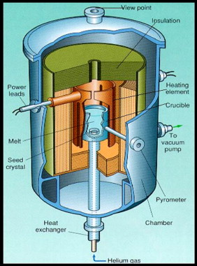
Figure 1. Schematic of a typical HEM furnace for Sapphire manufacture, consists of heating elements, thermal insulated furnace chamber, helium gas derived heat exchanger, and pyrometer and viewpoint-based observation system.
In a typical HEM process, a crucible is positioned on top of a heat exchanger. A monocrystalline seed is placed at the bottom center of the crucible, directly above the heat exchanger, while the amorphous or polycrystalline starting material is packed around and above the seed. As illustrated in Figure 2 (originally described by Viechnicki et al.[2]), the starting material melts initially, leaving the seed to act as a nucleation core. Heat is then directionally extracted from the melt through the seed, driving the crystallization process outward from the core to the surrounding liquid. To investigate this crystallization process in various materials, such as silicon and sapphire, numerical computations based on the Leibniz–Reynolds transport theorem have been widely employed. The general continuity equation is expressed as Equation 1, where $dV$ is the volume element, $dA$ is the surface area element, $f$ is the transport function, $v_{b}=v_{b}(x, t)$ is the boundary velocity of the area element, and $n$ is the outward unit normal vector. Over the past two decades, the integration of finite element methods and high-performance computing has significantly advanced these numerical investigations.
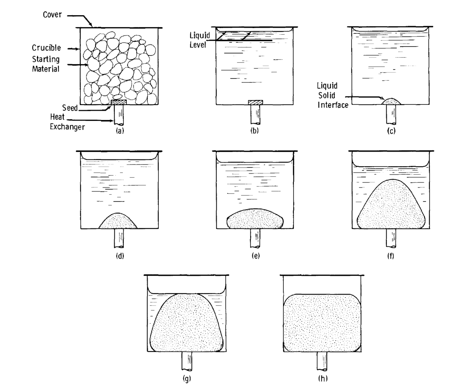
Figure 2. A typical HEM Process; a. status of crucible, cover, starting material, and seed prior to melting; b. starting material melted; c. seed partially melted for nucleation process; d. first stage of growth; e. second stage of growth covered bottom; f. third stage of interface expanding; g. fourth stage of growth liquid solid interface breaks liquid surface; h. crystal growth completed.
Eqn. 1. General continuous equations for Leibniz–Reynolds transport theorem
In addition to Sapphire and Silicon, High-melting sesquioxides (such as Sc2O3, Y2O3, and Lu2O3), Neighborite (NaMgF3), NBW (NaBiW2O8), NBP (Na5B2P3O13), Bismuth germanate, and Cadmium telluride, have been produced by HEM process.[3-8] The table 1 detailed listed materials can be growth by HEM method, and their supplementary equipment such as crucible and furnace.
Table 1. Materials can be growth by HEM method
| Materials | Crucibles | Protect gas | Reference |
|---|---|---|---|
| Bismuth germanate (Bi4Ge3O12, BGO) | Platinum | vacuum | Schmid et al. 3 |
| Cadmium telluride (CdTe) | Hexane | Argon | Baars et al.4 |
| Sodium–bismuth tungstate (NaBiW2O8; NBW) | unknown | vacuum | Rahab et al.5 |
| Sodium–phosphate (Na5B2P3O13; NBP) | unknown | vacuum | Rahab et al.5 |
| Yb-doped Lu2O3 (Yb:Lu2O3) | Rhenium | N2:H2 (0.9:0.1) | Peters et al.6 |
| Neighborite (NaMgF3) | unknown | vacuum | Oçafrain et al.7 |
| Sesquioxide of yttrium family | Rhenium | N2:H2 | Peters et al.8 |
CVD as a one of majority thin film and nanoscale crystalline synthesis method has a similar mechanism in thermodynamics and reaction kinetics with HEM. Specifically, similar mechanism applied in both heat up and crystalline process. The majority deference between two methods concentrated on the phase of materials. The HEM involved in a heating process from solid phase to liquid phase and a crystalline process from liquid phase. The engineering issues concentrated on the methods to calculating the latent heat and balancing the growth and evaporation under specific pressures. As well, the CVD involved in an evaporating process from solid phase to gas phase, a crystalline process from gas phase to solid, and a reaction involved two reactors (precursors). In addition, the reaction kinetics between precursor would be considered in all CVD process, as well would be considered in some specific HEM process of which growth material reacts with crucible materials such as the pair of silicon and quartz. Because of the similar growth mechanism, the computational analysis tool for HEM can be shared to CVD, such as the Leibniz–Reynolds transport theorem, therefore brings economics benefit as above mentioned.
Compared to HEM’s heating-growth two-step process, a typical thermal CVD has a slightly complex process including heating up, reaction, and growth. Specifically, a typical CVD process can be separated into three main stages; in first stage, gas phase reactant was vehicle to reactor by carrier gas and mix with precursor; in second stage, reactant react with precursor and forming products and by-products; in third stage, products deposited on the substrate forming the thin film and by-products vehicle out to the reactor by carrier gas. The process of deposition on substrate was considered as a crystalline process from gas phase directly. A typical thermal CVD system, which was depicted schematically in Figure 3 originally created by Sun et al.,[9] consists of gas delivery and vacuum systems, reaction furnace, energy source, an exhaust system, and control system.
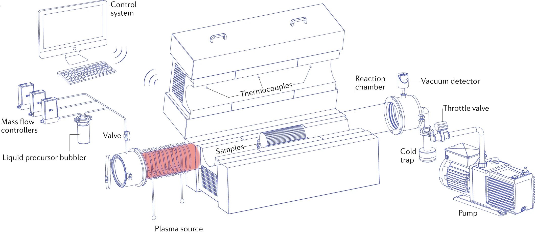
Figure 3. Schematic diagram of a typical thermal CVD system, gas delivery and vacuum systems, reaction furnace, energy source, an exhaust system, and control system.
Theoretically, CVD has less limitations in reactors and precursors than other nano crystalline methods; as well provided tunable ability to produces which significantly increased capacity in application. Therefore, most materials involved in surface reactions can be synthesized using CVD technique, such as silicon, sapphire, graphene, diamonds, TMD materials (such as molybdenum disulfide and tungsten disulfide), and polymers (such as PEDOT and Ppy). Their application covered nearly all research hotspot across from quantum computation to medical diagnosis. For example, carbon-based nanomaterials, such as diamond, graphene, and carbon nanotube, can be synthesized using CVD with precursors combination of alkenyl group and hydrogen. Further decreased manufacture pressure from super high (>5 GPa) to moderate pressure (<0.01 GPa) and manufacture temperature from over 1500°C to 900°C for diamond; as well the tunable ability reflected in the potential to produce graphene and carbon nanotube using same equipment with minus change in parameters.
Among those materials, TMDs was considered as one kind of most competitive candidates in several novel applications because of their physical properties such as direct band gap, heterostructures, and strong spin–orbit coupling. Those excellence properties promised their potential in high performance electronic components, photonic and optical and electrochemical sensing; their application includes flexible/transparent field-effect transistors, biosensors, color sensor, wavelength sensor, specific gas sensor. Molybdenum disulfide (MoS2) and tungsten disulfide (WS2) nanocrystals have been proved capability as photodetector and transistors. For example, Cheng et al. integrated MoS2 nano-transistors on quartz and flexible substrates to achieve a highly performance self-aligned device, Shokri et al. investigated electronic and transport properties of simple gas molecules such as CO and NO in monolayer MoS2 and theoretically revealed its potential as gas sensors, Bilgin et al. using CVD synthesized monolayer optoelectronic-grade molybdenum disulfide, and their follow-up research by Hejazi et al. proved the capability in precise wavelength measurement.[10-13] Moreover, Molybdenum diselenide (MoSe2) has been proved the identical potential in similar applications. Owing to its higher electrical conductivity from Se, MoSe2 has an even broader application in energy storage, photoelectronic, and electrocatalysis.[14] For example, Choi et al. discovered MoSe2 embedded CNT ball has ability in sodium-ion storage with excellence stability and reversible feature, which provided potential in battery applications; Tang et al. reported the hydrogen evolution reaction activity of MoSe2, which provided possibility to become electrocatalysis; Du et al. investigated the optical absorbance of monolayer MoSe2 in both computational and practical and provided theoretical support for photoelectronic.[15-17]
Funding
The authors gratefully acknowledge the funding support from the Young Scholar Foundation of the North China Institute of Aerospace Engineering and the equipment support from Shandong Finest Hour Technology Co., Ltd.
Conflicts of Interest
The authors declare that the research was conducted in the absence of any commercial or financial relationships that could be construed as a potential conflict of interest.
References
-
D. B. Joyce, F. Schmid. “Progress in the growth of large scale Ti:sapphire crystals by the heat exchanger method (HEM) for petawatt class lasers.” J. Cryst. Growth 2010, 312, 8, 1138–41.
-
D. Viechnicki, F. Schmid. “Crystal growth using the heat exchanger method (HEM).” J. Cryst. Growth 1974, 26, 1, 162–64.
-
F. Schmid, C. P. Khattak, M. B. Smith. “Growth of bismuth germanate crystals by the heat exchanger method.” J. Cryst. Growth 1984, 70, 1, 466–70.
-
C. P. Khattak, F. Schmid. “Growth of CdTe crystals by the heat exchanger method (HEMN).” 1989, 1106, 47–55.
-
H. Rahab, D. Ouadjaout, A. Manseri, O. Viraphong, J. P. Chaminade. “Growth by the heat exchanger method of NaBiW2O8 and Na5B2P3O13 crystals.” J. Cryst. Growth 2007, 303, 2, 629–31.
-
R. Peters, C. Kränkel, K. Petermann, G. Huber. “Crystal growth by the heat exchanger method, spectroscopic characterization and laser operation of high-purity Yb:Lu2O3.” J. Cryst. Growth 2008, 310, 7, 1934–38.
-
A. Oçafrain, J. P. Chaminade, O. Viraphong, R. Cavagnat, M. Couzi, M. Pouchard. “Growth by the heat exchanger method and characterization of neighborite, NaMgF3.” J. Cryst. Growth 1996, 166, 1, 414–18.
-
V. Peters, A. Bolz, K. Petermann, G. Huber. “Growth of high-melting sesquioxides by the heat exchanger method.” J. Cryst. Growth 2002, 237–239, 879–83.
-
L. Sun, G. Yuan, L. Gao, J. Yang, M. Chhowalla, M. H. Gharahcheshmeh, K. K. Gleason, Y. S. Choi, B. H. Hong, Z. Liu. “Chemical vapour deposition.” Nat. Rev. Methods Primers 2021, 1, 1, 5.
-
R. Cheng, S. Jiang, Y. Chen, Y. Liu, N. Weiss, H.-C. Cheng, H. Wu, Y. Huang, X. Duan. “Few-layer molybdenum disulfide transistors and circuits for high-speed flexible electronics.” Nat. Commun. 2014, 5, 1, 5143.
-
A. Shokri, N. Salami. “Gas sensor based on MoS2 monolayer.” Sens. Actuators, B 2016, 236, 378–85.
-
D. Hejazi, S. Liu, S. Ostadabbas, S. Kar. “Transition metal dichalcogenide thin films for precise optical wavelength estimation using bayesian inference.” ACS Appl. Nano Mater. 2019, 2, 7, 4075–84.
-
I. Bilgin, F. Liu, A. Vargas, A. Winchester, M. K. L. Man, M. Upmanyu, K. M. Dani, G. Gupta, S. Talapatra, A. D. Mohite, S. Kar. “Chemical vapor deposition synthesized atomically thin molybdenum disulfide with optoelectronic-grade crystalline quality.” ACS Nano 2015, 9, 9, 8822–32.
-
A. Eftekhari. “Molybdenum diselenide (MoSe2) for energy storage, catalysis, and optoelectronics.” Appl. Mater. Today 2017, 8, 1–17.
-
S. H. Choi, Y. C. Kang. “Fullerene-like MoSe2 nanoparticles-embedded CNT balls with excellent structural stability for highly reversible sodium-ion storage.” Nanoscale 2016, 8, 7, 4209–16.
-
H. Tang, K. Dou, C.-C. Kaun, Q. Kuang, S. Yang. “MoSe2 nanosheets and their graphene hybrids: synthesis, characterization and hydrogen evolution reaction studies.” J. Mater. Chem. A 2013, 2, 2, 360–64.
-
W. Du, P. Yu, J. Zhu, C. Li, H. Xu, J. Zou, C. Wu, Q. Wen, H. Ji, T. Liu, Y. Li, G. Zou, J. Wu, Z. M. Wang. “An ultrathin MoSe2 photodetector with near-perfect absorption.” Nanotechnology 2020, 31, 22, 225201.
-
C. P. Khattak, P. J. Guggenheim, F. Schmid. “Growth of 15-inch diameter sapphire boules.” 2003, 5078, 47–53.
-
C. P. Khattak, F. Schmid. “Growth of the world’s largest sapphire crystals.” J. Cryst. Growth 2001, 225, 2, 572–79.
-
H. Zhang, L. Zheng, X. Ma, B. Zhao, C. Wang, F. Xu. “Nucleation and bulk growth control for high efficiency silicon ingot casting.” J. Cryst. Growth 2011, 318, 1, 283–87.
-
C. Reimann, M. Trempa, T. Jung, J. Friedrich, G. Müller. “Modeling of incorporation of O, N, C and formation of related precipitates during directional solidification of silicon under consideration of variable processing parameters.” J. Cryst. Growth 2010, 312, 7, 878–85.
-
M. Srinivasan, P. Ramasamy. “Computational modeling on the influence of the schmidt number on second phase impurities SiC, Si2N2O and Si3N4 in grown mc-silicon for PV applications.” Silicon 2018, 10, 3, 1077–85.
-
M. Trempa, C. Reimann, J. Friedrich, G. Müller, D. Oriwol. “Mono-crystalline growth in directional solidification of silicon with different orientation and splitting of seed crystals.” J. Cryst. Growth 2012, 351, 1, 131–40.
-
J. Wei, H. Zhang, L. Zheng, C. Wang, B. Zhao. “Modeling and improvement of silicon ingot directional solidification for industrial production systems.” Sol. Energy Mater. Sol. Cells 2009, 93, 9, 1531–39.
-
C. W. Lan, W. C. Lan, T. F. Lee, A. Yu, Y. M. Yang, W. C. Hsu, B. Hsu, A. Yang. “Grain control in directional solidification of photovoltaic silicon.” J. Cryst. Growth 2012, 360, 68–75.
-
D. Zhu, L. Ming, M. Huang, Z. Zhang, X. Huang. “Seed-assisted growth of high-quality multi-crystalline silicon in directional solidification.” J. Cryst. Growth 2014, 386, 52–56.
-
M. Srinivasan, P. Karuppasamy, P. Ramasamy, A. K. Barua. “Numerical modelling on stress and dislocation generation in multi-crystalline silicon during directional solidification for PV applications.” Electron. Mater. Lett. 2016, 12, 4, 431–38.
-
D. R. Baer. “The chameleon effect: characterization challenges due to the variability of nanoparticles and their surfaces.” Front. Chem. 2018, 6.
-
K. K. H. Smithe, S. V. Suryavanshi, M. Muñoz Rojo, A. D. Tedjarati, E. Pop. “Low variability in synthetic monolayer MoS2 devices.” ACS Nano 2017, 11, 8, 8456–63.
-
T. K. Patra, F. Zhang, D. S. Schulman, H. Chan, M. J. Cherukara, M. Terrones, S. Das, B. Narayanan, S. K. R. S. Sankaranarayanan. “Defect dynamics in 2-D MoS2 probed by using machine learning, atomistic simulations, and high-resolution microscopy.” ACS Nano 2018, 12, 8, 8006–16.
-
S. Hong, K. Nomura, A. Krishnamoorthy, P. Rajak, C. Sheng, R. K. Kalia, A. Nakano, P. Vashishta. “Defect healing in layered materials: a machine learning-assisted characterization of MoS2 crystal phases.” J. Phys. Chem. Lett. 2019, 10, 11, 2739–44.
-
X. Dong, H. Li, Z. Jiang, T. Grünleitner, İ. Güler, J. Dong, K. Wang, M. H. Köhler, M. Jakobi, B. H. Menze, A. K. Yetisen, I. D. Sharp, A. V. Stier, J. J. Finley, A. W. Koch. “3D deep learning enables accurate layer mapping of 2D materials.” ACS Nano 2021, 15, 2, 3139–51.